
Terminal device antenna device and implementation method thereof

A technology of terminal equipment and antenna device, which is applied in the direction of antenna grounding device, antenna support/installation device, and device that enables antennas to work in different bands at the same time. It can solve the problems that multiple broadband bands cannot work at the same time, and improve Effect of EMC Characteristics

Active Publication Date: 2019-12-03
ZTE CORP
View PDF16 Cites 1 Cited by
  • Summary
  • Abstract
  • Description
  • Claims
  • Application Information

AI Technical Summary

Problems solved by technology

[0006] An antenna device and implementation method for terminal equipment provided by the embodiments of the present invention solve the problem in the prior art that multiple wide frequency bands cannot work simultaneously in a limited size

Method used


Image

  • Terminal device antenna device and implementation method thereof
  • Terminal device antenna device and implementation method thereof
  • Terminal device antenna device and implementation method thereof

Examples


Embodiment 1

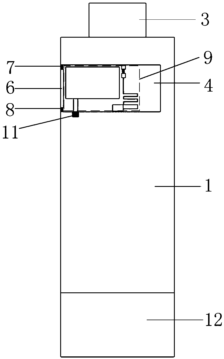
[0064] FIG. 3 is a schematic structural diagram of an antenna device of a terminal device provided by an embodiment of the present invention. As shown in FIG. 3 , it includes a top-layer metal ground 1 . The bottom metal ground 2 is located on the bottom surface of the motherboard 12 . The main board 12 of the antenna terminal equipment is made of non-metallic material, and the metal area of ​​the main board 12 of the terminal equipment includes multiple printed circuit layers. The USB interface 3 is connected with other digital devices.

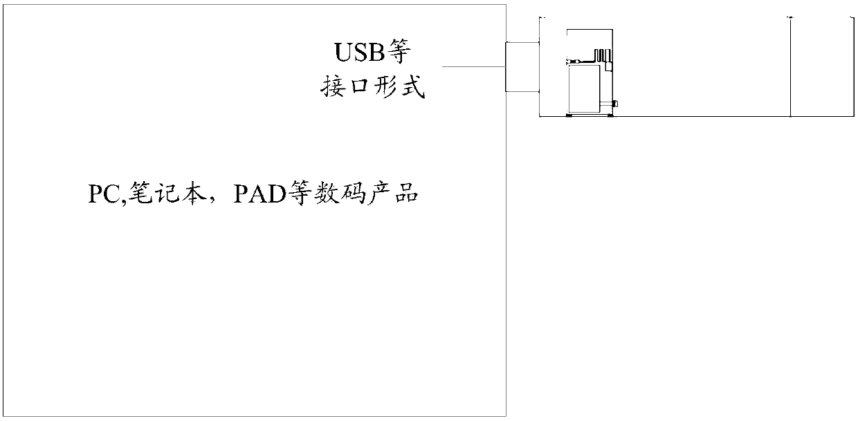
[0065] The antenna topology unit 9 is laid around the top non-metal area 4 of the top metal ground 1 and the bottom non-metal area 5 of the bottom metal ground 2 of the main board 12 of the terminal device. Wherein the top non-metallic region 4 and the bottom non-metallic region 5 can be any regular or irregular shape such as square, circle, rhombus, trapezoid, triangle, etc., and are not limited to this embodiment figure 2 The shown rect...

Embodiment 2

[0071] Figure 5 It is a schematic diagram of the antenna structure of the second terminal equipment provided by the implementation example of the present invention, as shown in Figure 5 As shown, the difference between this embodiment and Embodiment 1 is that a metal coupling sheet 13 is provided on the third radiator 93 on the top layer of the antenna, and a non-metallic medium between the printed layers is used between the metal coupling sheet 13 and the antenna radiator Or air medium for coupling. There is a gap between the metal coupling sheet 13 and the data card main board 12 , through which the metal coupling sheet 13 is coupled to the data card main board 12 , so as to realize the secondary coupling between the antenna radiator and the data card main board 12 .

[0072] As shown in FIG. 3 , the antenna topology unit 9 is laid around the top non-metallic area 4 of the top metal ground 1 and the bottom non-metallic area 5 of the bottom metal ground 2 of the main board...

Embodiment 3

[0077] Figure 6 It is a schematic diagram of the antenna structure of the third terminal equipment provided by the implementation example of the present invention, as shown in Figure 6 As shown, the difference between this embodiment and Embodiment 1 is that: a metal coupling piece 14 is arranged in the non-metallic region 5 of the bottom layer of the antenna, and the metal coupling piece 14 is arranged on the non-metallic region by printing or welding. There is a gap between the metal coupling sheet 14 and the data card main board 12 , through which the metal coupling sheet 14 is coupled to the data card main board 12 , so as to realize the secondary coupling between the antenna radiator and the data card main board 12 .

[0078] As shown in FIG. 3 , the antenna topology unit 9 is laid around the top non-metallic area 4 of the top metal ground 1 and the bottom non-metallic area 5 of the bottom metal ground 2 of the main board 12 of the terminal device. Wherein the top non-...


PUM


Abstract

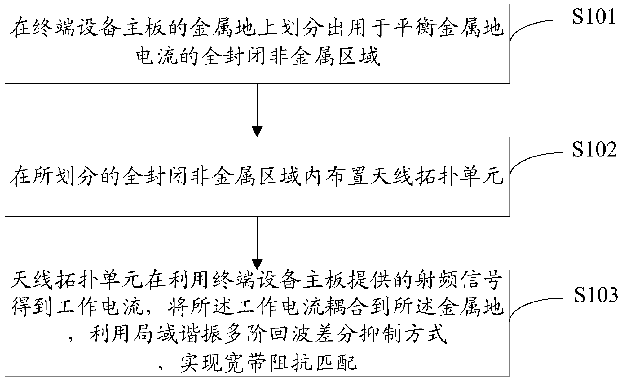
The invention discloses a terminal device antenna device and an implementation method thereof, and relates to the field of antennae. The method comprises the steps of: dividing a metal ground of a terminal device mainboard into a totally-enclosed non-metal region for balancing the current of the metal ground; and arranging an antenna topology unit in the divided totally-enclosed non-metal region,wherein the antenna topology unit obtains a working current by using a radio frequency signal provided by the terminal device mainboard, couples the working current to the metal ground, and achieves broadband impedance matching by using a local resonance multi-order echo differential suppression mode. According to the embodiment of the invention, the technical problem in the prior art that a plurality of wide frequency bands cannot work at the same time under a limited size is solved, and the electromagnetic compatibility characteristic is greatly improved.

Description

technical field [0001] The present invention relates to the field of antennas, in particular to an antenna device for terminal equipment and an implementation method. Background technique [0002] Most existing wireless mobile terminals use antennas such as monopole antennas, planar inverted-F antennas (Planar Inverted-FAntenna, PIFA), and loop antennas. If these antennas need to meet the required frequency band coverage, their physical size will be large, and the bandwidth of a single type of antenna cannot meet the working requirements of wireless mobile terminal communications. At present, for the antenna design to cover the Long Term Evolution (Long Term Evolution, LTE) frequency band, not only the antenna performance such as return loss, gain and efficiency of the antenna is required to be good, but also the size of the antenna is required to be as small as possible. According to the principle of the antenna, the size of the traditional antenna needs to be 1 / 2 or 1 / 4 o...

Claims


Application Information

Patent Timeline
IPC IPC(8): H01Q1/36H01Q1/48H01Q1/24
CPCH01Q1/36H01Q1/48H01Q1/243H01Q5/328H01Q5/314
Inventor 周闯柱王小明翁子彬
Owner ZTE CORP
Learn More