Anti-interference and overload-resistant MEMS accelerometer

A technology of accelerometer and sensitive structure, which is applied in the direction of measuring acceleration, speed/acceleration/shock measurement, measuring device, etc. It can solve the problems of application limitation, anti-interference, and lack of overload resistance, so as to improve anti-interference ability and enhance endurance. The effect of overload capacity and rigidity improvement

Active Publication Date: 2019-12-13
EAST CHINA INST OF OPTOELECTRONICS INTEGRATEDDEVICE
View PDF19 Cites 0 Cited by
  • Summary
  • Abstract
  • Description
  • Claims
  • Application Information

AI Technical Summary

Problems solved by technology

[0003] At present, foreign high-performance MEMS accelerometer products are relatively mature and have been widely used in many aspects. Domestic high-performance MEMS accelerometers have been deeply researched and developed, and some companies or laboratories have prepared high-precision single-axis accelerometers. Or multi-axis accelerometer products, but they are lacking in anti-interference and overload resistance, which limits their application in high-impact environments

Method used


Image

  • Anti-interference and overload-resistant MEMS accelerometer
  • Anti-interference and overload-resistant MEMS accelerometer
  • Anti-interference and overload-resistant MEMS accelerometer

Examples


Embodiment Construction

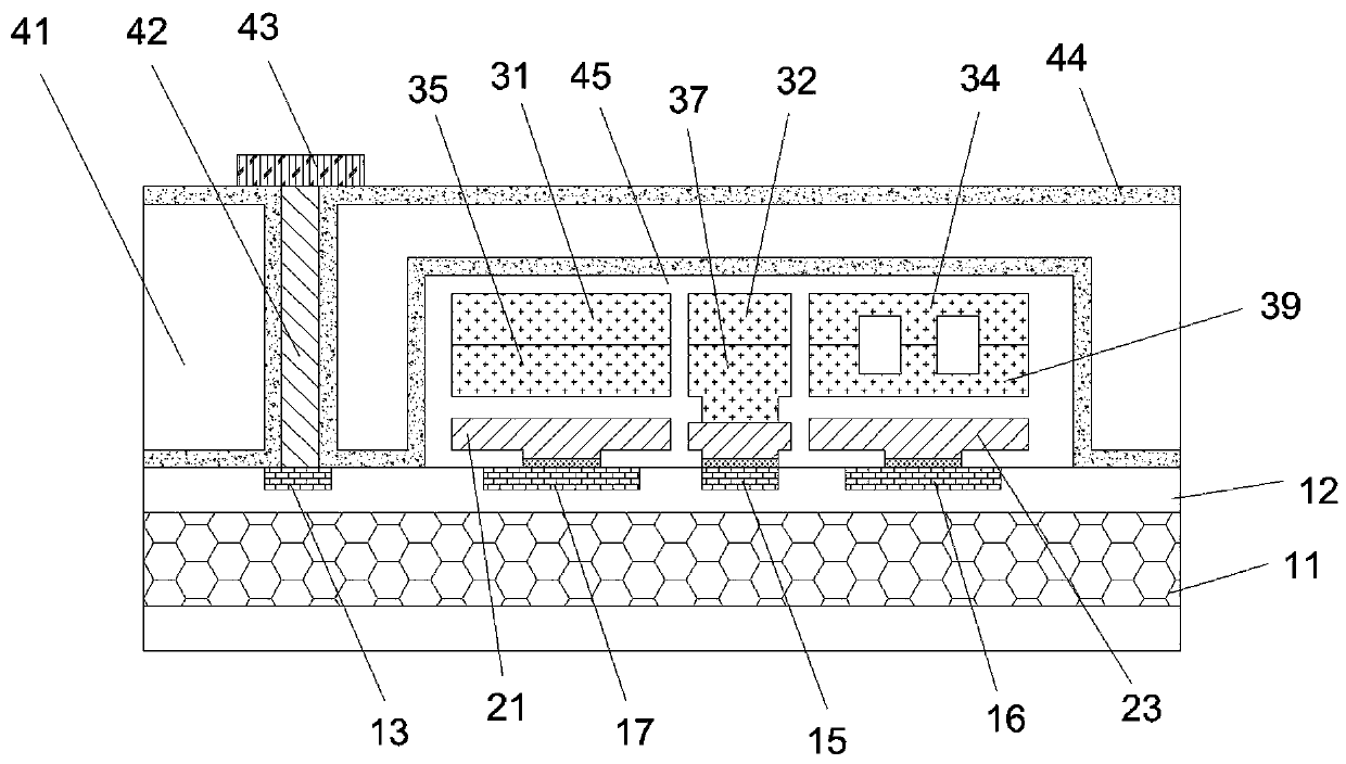
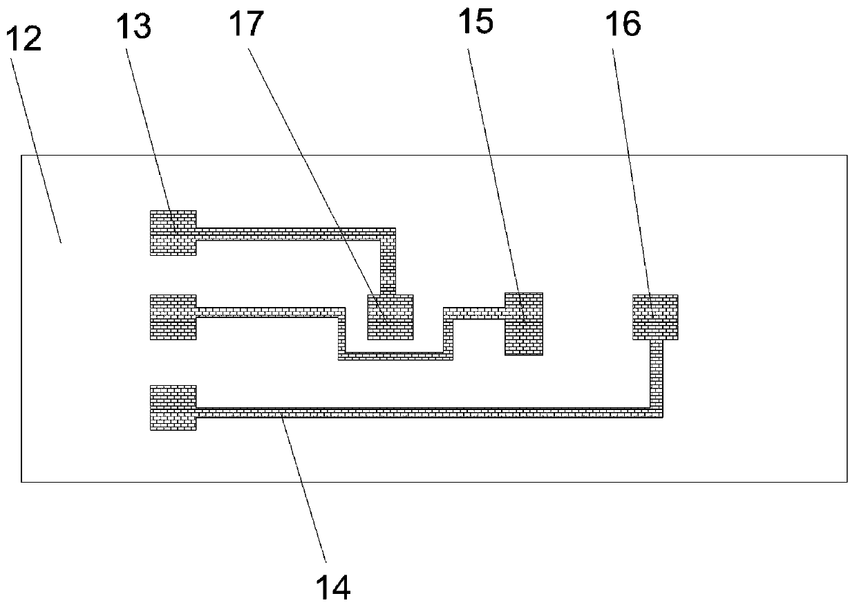
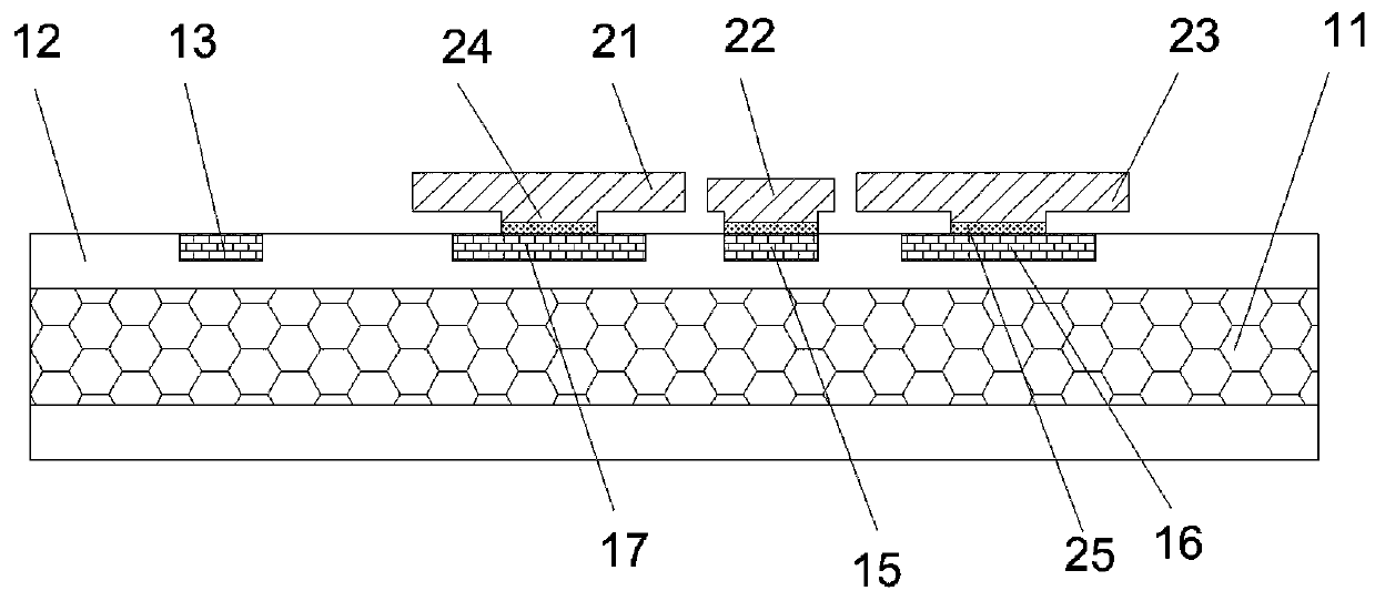
[0020] combine figure 1 and figure 2 As shown, the present invention provides an anti-jamming and overload-resistant MEMS accelerometer, comprising a sequentially bonded substrate layer, an induction electrode layer, a movable sensitive structure layer and a cap, and the substrate 11 of the substrate layer is provided with an insulating medium layer 12, a metal Copper PAD point 13, metal copper center anchor point 15, left metal copper anchor point 17 and right metal copper anchor point 16 located on both sides of metal copper center anchor point 15, metal copper center anchor point 15, left metal copper anchor point 17 and The right metal copper anchor points 16 are respectively connected to the metal copper PAD points 13 through the metal copper lead wires 14 .

[0021] combine image 3 and Figure 4 As shown, the sensing electrode layer includes a sensing electrode central anchor point 22, a left sensing electrode 21, and a right sensing electrode 23. The bottoms of the...


PUM


Abstract

The invention discloses an anti-interference and overload-resistant MEMS (Micro-Electro-Mechanical System) accelerometer. The accelerometer comprises a substrate layer, an induction electrode layer, amovable sensitive structure layer and a cap which are bonded in sequence. The induction electrode layer comprises an induction electrode center anchor point and induction electrodes on the two sides.The movable sensitive structure layer comprises a first movable sensitive structure center anchor point, a first solid movable sensitive structure and a first hollow movable sensitive structure. A silicon support column is arranged at the bottom of each induction electrode. The top end of each silicon support column is connected with the corresponding induction electrode, and the bottom end of each silicon support column is connected with the substrate layer. A second movable sensitive structure central anchor point, a second solid movable sensitive structure and a second hollow movable sensitive structure are respectively and symmetrically bonded above the first movable sensitive structure central anchor point, the first solid movable sensitive structure and the first hollow movable sensitive structure. A closed cavity is formed between the first hollow movable sensitive structure and the second hollow movable sensitive structure. The influence of the external environment on the performance of the device can be reduced, and the reliability of the device can be improved.

Description

technical field [0001] The invention relates to the technical field of micro-mechanical electronics, in particular to an anti-interference and overload-resistant MEMS accelerometer. Background technique [0002] MEMS (Micro-Electro-Mechanical Systems) is the abbreviation of Micro-Electro-Mechanical Systems. MEMS manufacturing technology uses micro-nano processing technology, especially the related technology of semiconductor wafer manufacturing, to manufacture various micro-nano mechanical structures, combined with dedicated control integration Circuits (ASIC), composed of intelligent micro-sensors, micro-actuators, micro-optical devices and other MEMS components. MEMS components have the advantages of small size, low cost, high reliability, low power consumption, high degree of intelligence, easy calibration, and easy integration, and are widely used in aerospace, medical, industrial production and various consumer products . [0003] At present, foreign high-performance ...

Claims


Application Information

Patent Timeline
Patent Type & Authority Applications(China)
IPC IPC(8): G01P15/125
CPCG01P15/125
Inventor 王鹏陈慧斌何凯旋黄斌王帆
Owner EAST CHINA INST OF OPTOELECTRONICS INTEGRATEDDEVICE
Why Eureka
Try Eureka