Schottky diode and manufacturing method thereof

A Schottky diode and electrode technology, which is applied in semiconductor/solid-state device manufacturing, electrical components, circuits, etc., can solve the problems of reduced conduction capacity and increased forward voltage of anti-surge capability

Active Publication Date: 2019-12-13
山东天岳电子科技有限公司
View PDF15 Cites 5 Cited by
  • Summary
  • Abstract
  • Description
  • Claims
  • Application Information

AI Technical Summary

Problems solved by technology

[0005] The embodiment of the present application provides a Schottky diode and its manufacturing method, aiming to solve the problem of increasing the forw

Method used


Image

  • Schottky diode and manufacturing method thereof
  • Schottky diode and manufacturing method thereof
  • Schottky diode and manufacturing method thereof

Examples


Embodiment Construction

[0027] In order to explain the overall concept of the present application more clearly, the following detailed description will be given by way of examples in combination with the accompanying drawings.

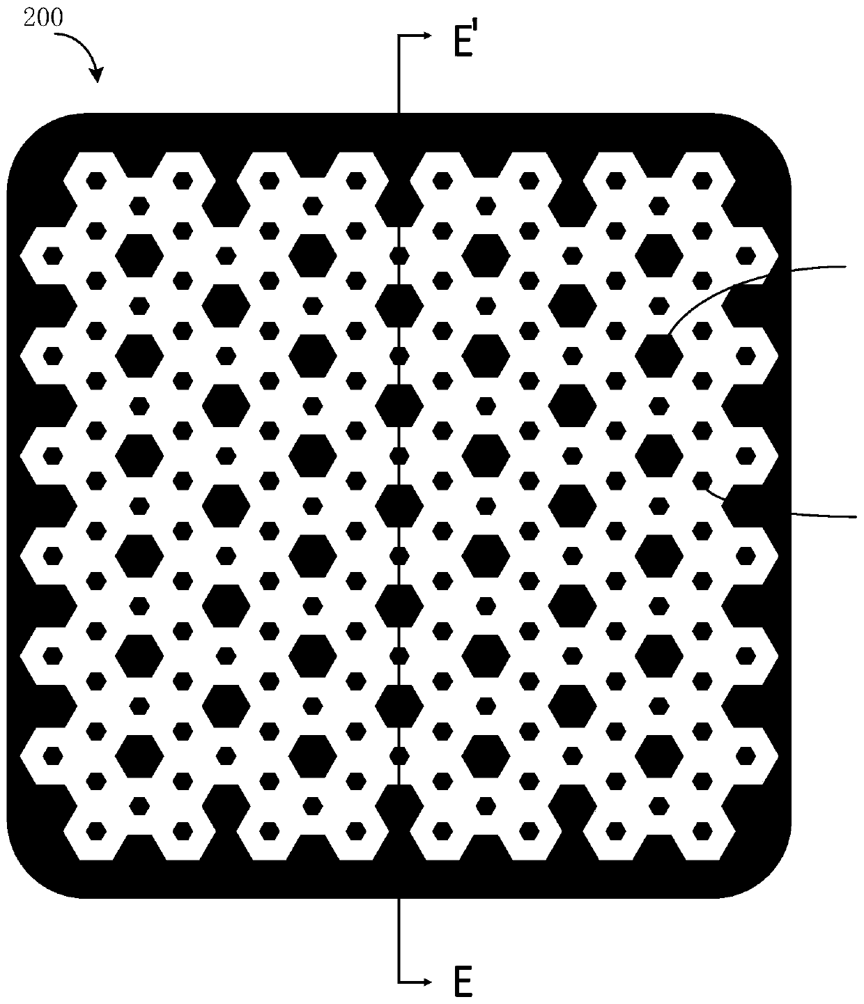
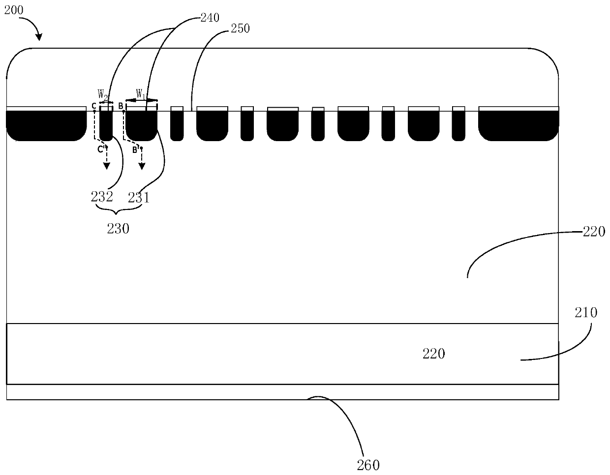
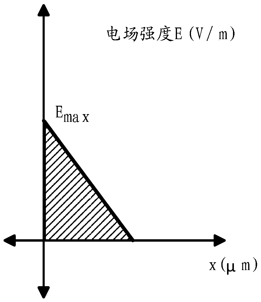
[0028] Schottky diodes in the prior art, in the case of normal current conduction, only Schottky participates in conduction, so the improvement of normal current conduction performance depends on the ratio of the Schottky junction area to the total area of ​​the Schottky diode , the larger the proportion of the Schottky junction area to the total area of ​​the Schottky diode, the better the forward conduction performance. In the case of a surge current impact, the voltage drop of the existing Schottky diode generally exceeds the built-in potential of the PN junction, causing the PN junction to be turned on, and the conductance modulation effect formed by the minority carrier injection of the PN junction can Reduce the resistance and conduction voltage drop of the device. Ther...


PUM


Abstract

The embodiment of the invention provides a Schottky diode and a manufacturing method thereof. The Schottky diode comprises an epitaxial layer with a first conductivity type. A plurality of semiconductor regions of a second conductivity type are arranged on the epitaxial layer, and the first conductivity type is different from the second conductivity type. The plurality of semiconductor regions ofthe second conductivity type comprise a plurality of first regions and a preset number of second regions which are uniformly surrounded by taking the first regions as centers. The width of the first region is greater than that of the second region, the depth of the first region is the same as that of the second region, and the shapes of ohmic contact regions formed by the first region and the second region are the same. And the first region and the second region respectively form PN junctions of the Schottky diode with the epitaxial layer. Through the technical scheme, the surge current resistance of the device can be enhanced under the condition in which the normal conduction performance of the Schottky diode in a normal current conduction mode is kept or not influenced as much as possible.

Description

technical field [0001] The invention relates to a semiconductor device, in particular to a Schottky diode and a manufacturing method thereof. Background technique [0002] Schottky diodes are widely used because of their low forward voltage and short reverse recovery time. However, the anti-surge capability of the Schottky diode is poor. In the case of a surge current, the Schottky diode may experience excessive instantaneous energy and temperature rise, which will cause the Schottky diode to fail. [0003] In order to solve the above problems, a kind of Schottky diode in the prior art, in the epitaxial layer of the Schottky diode, several semiconductor regions different from the conductivity of the epitaxial layer are arranged to increase the anti-surge capability of the Schottky diode . The wider the width of the semiconductor region, the stronger the surge resistance of the Schottky diode. However, the wider the width of the semiconductor region, the higher the forward...

Claims


Application Information

Patent Timeline
IPC IPC(8): H01L29/872H01L29/06H01L21/329
CPCH01L29/872H01L29/66143H01L29/0615H01L29/0688
Inventor 任娜
Owner 山东天岳电子科技有限公司
Why Eureka
Try Eureka