A kind of silicon pole plate and preparation method thereof
A technology of electrode plates and silicon wafers, applied in the field of silicon materials, can solve the problems of complex preparation process, poor electrical conductivity, low power density, etc., and achieve the effects of strong corrosion resistance, light weight and good power density
- Summary
- Abstract
- Description
- Claims
- Application Information
AI Technical Summary
Problems solved by technology
Method used
Image
Examples
Embodiment 1
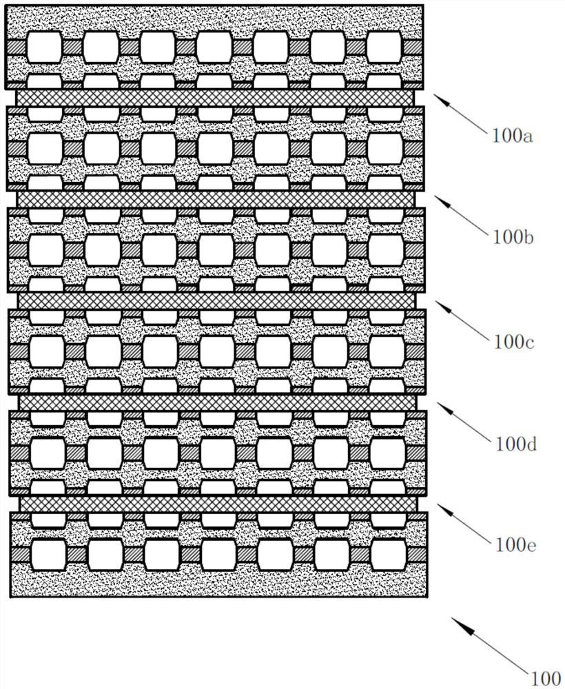
[0062] See figure 1 A fuel cell stack structure 100 is shown. The stack structure 100 includes fuel cell units connected in series and stacked together, and the number is not less than three. Specifically, in this embodiment, the number of fuel cell units 5; preferably, the output power of the electric stack structure 100 is not less than 0.1KW, of course, in other embodiments of the present invention, those skilled in the art can completely according to the required power requirements of the product field that actually needs to be applied, to select the number of fuel cell units, which is not specifically limited in the present invention.
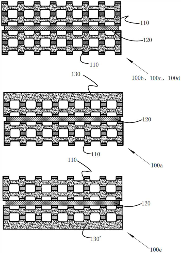
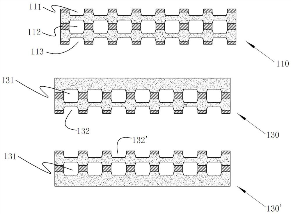
[0063] Such as figure 1 As shown, the stack structure of this embodiment 1 includes end fuel cell units 100a, 100e located at both ends and three middle fuel cell units 100b, 100c, 100d located in the middle, and each fuel cell unit includes sequentially stacked as a whole The anode plate, the anode electrode, the electrolyte diaphragm, ...
Embodiment 2
[0102] The rest of the technical solutions of this embodiment 2 are the same as those of embodiment 1, the difference is that in this embodiment 2, the silicon wafer adopts phosphorus-doped or boron-doped single crystal or polycrystalline silicon wafer, preferably, the resistivity range of the silicon wafer is 0.0005-0.05Ω.cm; see Figure 6 As shown, the preparation method of the middle silicon pole plate 210 includes the following steps:
[0103] B10), preparing the first silicon wafer and the second silicon wafer;
[0104] B20), respectively fabricating the first internal cooling medium channel on the reverse side, the reducing agent channel 211 on the front side, and the first inlet and outlet combination on both sides of the first silicon wafer by laser technology, and fabricating respectively on both sides of the second silicon wafer The combination of the second internal cooling medium channel on the front side, the oxidant channel 213 on the back side, and the second i...
Embodiment 3
[0109] The rest of the technical solutions of this embodiment 3 are the same as those of embodiment 1, the difference is that in this embodiment 3, the silicon chip is a single crystal or polycrystalline silicon chip doped with phosphorus or boron, preferably, the resistivity range of the silicon chip is 0.0005-0.05Ω.cm; see Figure 7 As shown, the preparation method of the middle silicon pole plate 310 includes the following steps:
[0110] C10), preparing the first silicon wafer and the second silicon wafer;
[0111] C20), directly using screen printing process (also called positive plastic process) to make conductive material layer 316 on both sides of the first silicon chip and the second silicon chip respectively, through the formation of conductive material layer 316, and then the first silicon The sheet can directly form the first inner cooling medium flow channel on the reverse side and the reducing agent flow channel 311 on the front side, and the second silicon chip...
PUM
| Property | Measurement | Unit |
|---|---|---|
| electrical resistivity | aaaaa | aaaaa |
| thickness | aaaaa | aaaaa |
| size | aaaaa | aaaaa |
Abstract
Description
Claims
Application Information


