
Plasma apparatus, semiconductor manufacturing method, and gas transport source

A plasma and plasma technology, applied in the field of plasma equipment, can solve the problems of increasing the complexity of manufacturing and production of integrated circuits, increasing the production efficiency, reducing the manufacturing cost, etc., to achieve the best sealing effect and the effect of eliminating leakage

Active Publication Date: 2019-12-20
TAIWAN SEMICON MFG CO LTD
View PDF10 Cites 0 Cited by
  • Summary
  • Abstract
  • Description
  • Claims
  • Application Information

AI Technical Summary

Problems solved by technology

Generally speaking, this kind of manufacturing process with reduced size can provide the benefits of increasing production efficiency and reducing manufacturing costs. However, this kind of manufacturing process with reduced size will also increase the complexity of manufacturing and producing integrated circuits.

Method used


Image

  • Plasma apparatus, semiconductor manufacturing method, and gas transport source
  • Plasma apparatus, semiconductor manufacturing method, and gas transport source
  • Plasma apparatus, semiconductor manufacturing method, and gas transport source

Examples


Embodiment Construction

[0075]The implementation modes or examples disclosed below are used to illustrate or complete various technical features of the present invention, and the specific embodiments of the described elements and configurations are used to simplify the description of the present invention, so as to make the disclosure more thorough and complete. In order to fully convey the scope of this disclosure to those of ordinary skill in the art. Of course, the present disclosure can also be implemented in many different forms without being limited to the embodiments described below. For example, if it is described in the embodiment that a first feature is formed on or above a second feature, it may include that the above-mentioned first feature is in direct contact with the above-mentioned second feature, or may include Additional features are formed between the first feature and the second feature such that the first feature and the second feature are not in direct contact. In addition, the...


PUM


Abstract

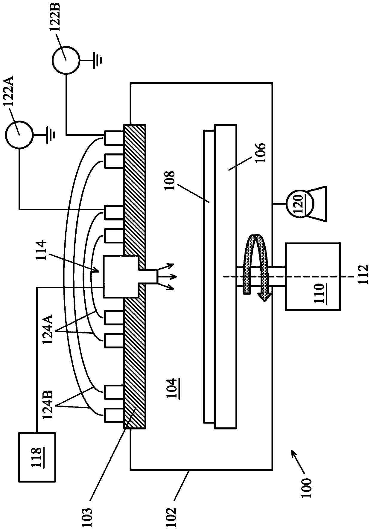
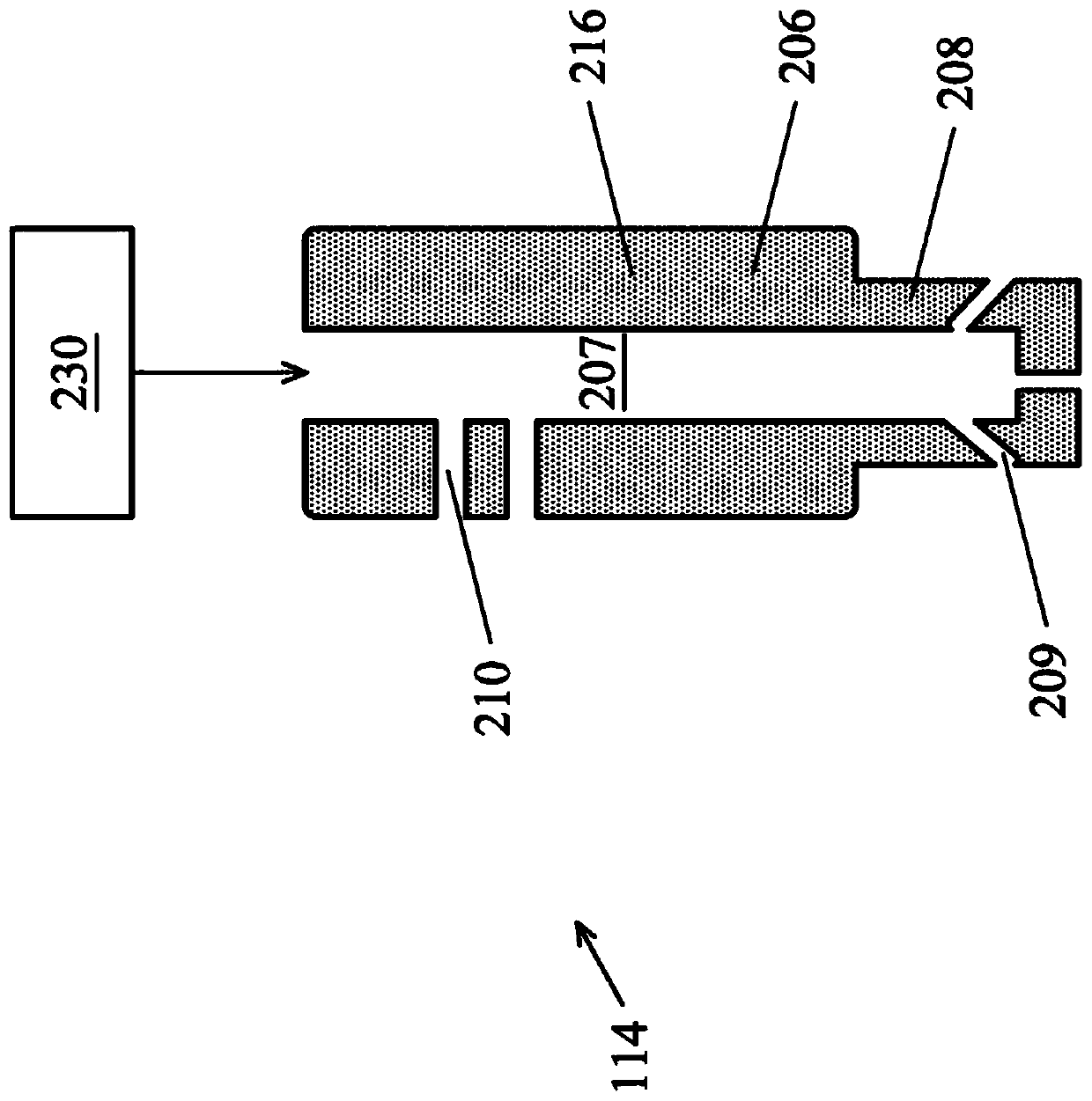
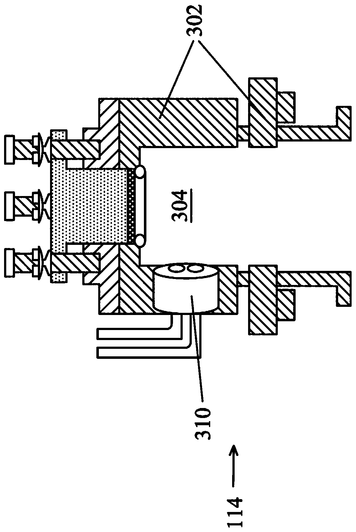
The invention provides a plasma apparatus, a semiconductor manufacturing method, and a gas transport source. The plasma apparatus includes chamber walls and a chamber window defining an enclosed space. A chamber window is disposed between a plasma antenna and a substrate support. A gas delivery source is mechanically coupled to the chamber window. The gas delivery source comprises a gas injector having a passageway, a window at a first end of the passageway, and a nozzle at a second end of the passageway. The nozzle of the gas delivery source is disposed in the enclosed space. A fastening device is mechanically coupled to the gas delivery source. The fastening device is adjustable to adjust a sealing force against the gas injector.

Description

technical field [0001] The present disclosure relates to a plasma device, a semiconductor manufacturing method, and a gas delivery source. Background technique [0002] In recent years, semiconductor integrated circuits have experienced exponential growth. Technological advances in integrated circuit materials and design have resulted in generations of integrated circuits, with each generation having smaller and more complex circuits than the previous generation. During the development of integrated circuits, when the geometric size (that is, the smallest element or line that can be produced in the manufacturing process) shrinks, the functional density (that is, the number of interconnect devices per chip area) Usually increases. Generally speaking, such size reduction manufacturing process can provide benefits of increasing production efficiency and reducing manufacturing cost. However, such size reduction manufacturing process will also increase the complexity of manufac...

Claims


Application Information

Patent Timeline
IPC IPC(8): H01J37/32H01L21/67
CPCH01J37/3244H01J37/32513H01L21/67069H01J2237/3341H01J37/3211H01J37/32715H01J37/32963H01L21/67167H01L21/67201H01L22/26H01L21/6831H01L21/3065H01L21/31116H01L21/31138H01L21/32136H01J2237/334H01J2237/20214
Inventor 许泳顺张景郁张乔凯谢伟康林建坊
Owner TAIWAN SEMICON MFG CO LTD
Learn More