Shield gate field effect transistor and manufacturing method thereof
A technology of field effect transistors and shielding gates, which is applied in semiconductor/solid-state device manufacturing, semiconductor devices, electrical components, etc., to achieve the effect of free adjustment of capacitance
- Summary
- Abstract
- Description
- Claims
- Application Information
AI Technical Summary
Problems solved by technology
Method used
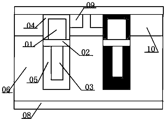
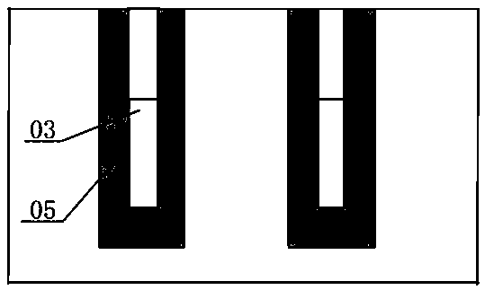
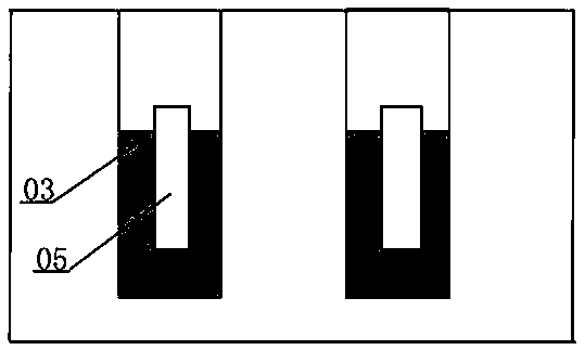
Image

Examples
Embodiment Construction
[0034] In order to enable those skilled in the art to better understand the solution of the present application, the technical solution in the embodiment of the application will be clearly and completely described below in conjunction with the accompanying drawings in the embodiment of the application. Obviously, the described embodiment is only It is an embodiment of a part of the application, but not all of the embodiments. Based on the embodiments in this application, all other embodiments obtained by persons of ordinary skill in the art without creative efforts shall fall within the scope of protection of this application.
[0035] It should be noted that the terms "first" and "second" in the description and claims of the present application and the above drawings are used to distinguish similar objects, but not necessarily used to describe a specific sequence or sequence. It is to be understood that the data so used are interchangeable under appropriate circumstances such...
PUM
 Abstract
Description
Claims
Application Information
 - R&D
- Intellectual Property
- Life Sciences
- Materials
- Tech Scout
- Unparalleled Data Quality
- Higher Quality Content
- 60% Fewer Hallucinations
Browse by: Latest US Patents, China's latest patents, Technical Efficacy Thesaurus, Application Domain, Technology Topic, Popular Technical Reports.
© 2025 PatSnap. All rights reserved.Legal|Privacy policy|Modern Slavery Act Transparency Statement|Sitemap|About US| Contact US: help@patsnap.com