Preparation method of silicon through hole interconnection structure

An interconnection structure and through-silicon via technology, which is applied in the manufacture of semiconductor/solid-state devices, electrical components, and electrical solid-state devices, can solve problems such as high cost, poor reliability of through-silicon via interconnection structures, and cumbersome preparation processes, and achieve good results. Reliability, reduction of preparation time and cost, effect of reduction of preparation steps

Inactive Publication Date: 2020-01-03
NAT CENT FOR ADVANCED PACKAGING
View PDF5 Cites 2 Cited by
  • Summary
  • Abstract
  • Description
  • Claims
  • Application Information

AI Technical Summary

Benefits of technology

This patented process allows for efficient production of reliable semiconductor structures with improved performance compared to existing methods such as wirebonds and solder connections. It involves laminated layers made up of multiple devices joined together without any space left behind after being processed. By doing these processes before connecting them into final products, it simplifies the overall fabrications process while reducing costs associated with equipment maintenance. Additionally, the use of specific techniques like lasers makes possible precise placement of conductive elements within certain areas, resulting in increased efficiency and reduced defect rates. Overall, this new technique improves the quality control and speedup of producing electronic circuits with good electrical properties.

Problems solved by technology

The technical problem addressed in this patented text relates to achieving efficient production of highly integrated semiconductor packages while reducing impedance caused by increased signal transmission due to multiple connections perpendicular to each other. This requires that certain areas within the package have more conductive paths than others for better current flowing or improved device function. Current methods like chemical vapor deposition require long periods of time before being able to fully fill all these spaces without causing issues.

Method used


Image

  • Preparation method of silicon through hole interconnection structure
  • Preparation method of silicon through hole interconnection structure
  • Preparation method of silicon through hole interconnection structure

Examples


Embodiment 1

[0058] This embodiment provides a method for preparing a through-silicon via interconnection structure, including the following steps,

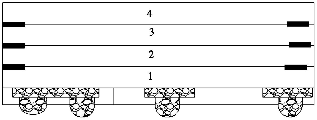
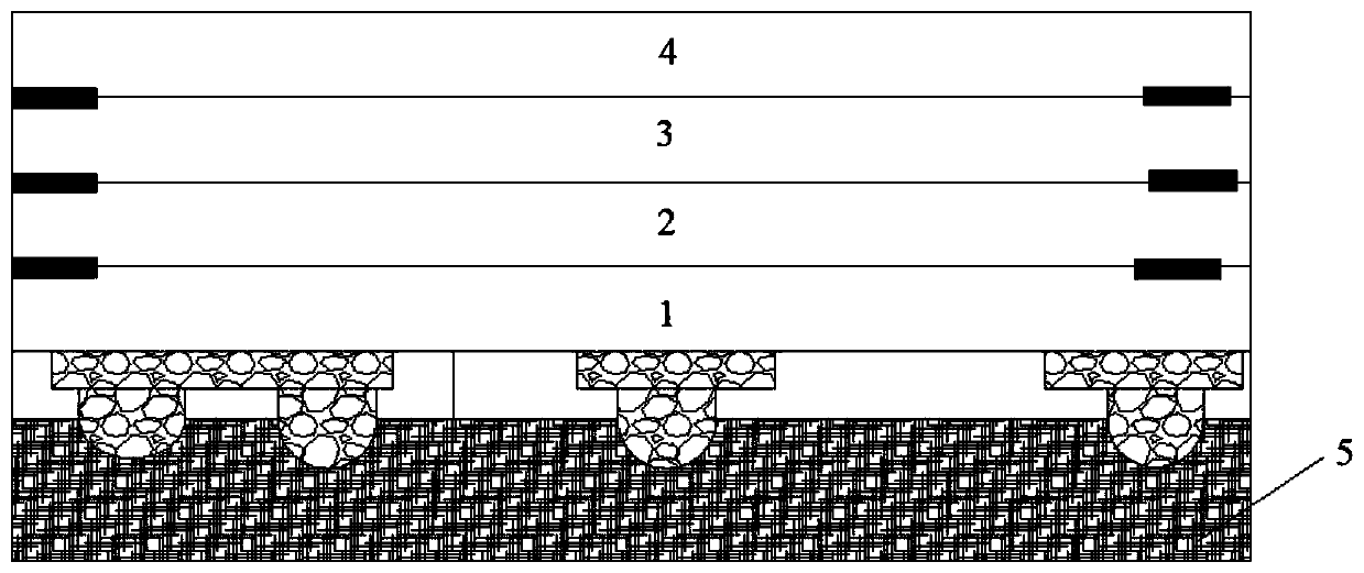
[0059] Using the mounting process, the first device, the second device, the third device and the fourth device are respectively bonded, such as figure 1 shown, and then use a temporary bonding glue to bond a carrier sheet on the bottom, such as figure 2 shown;

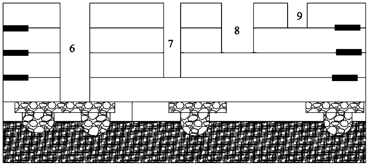
[0060] Use dry etching technology to etch to obtain 4 silicon holes (i.e. the first silicon hole 6, the second silicon hole 7, the third silicon hole 8 and the fourth silicon hole 9, the depths of which are respectively the stacked thickness of the four devices , the stacked thickness of three devices, the stacked thickness of two devices, and the stacked thickness of one device. When etching silicon holes, the etching sequence is from shallow to deep. When etching deeper holes, use dry film to The etched shallow holes are covered and protected, and then the deep holes are etched. ...

Embodiment 2

[0065] This embodiment provides a method for preparing a through-silicon via interconnection structure, including the following steps,

[0066] Bond the first device, the second device, the third device and the fourth device respectively by using the SMT process, and then use a temporary bonding glue to bond a carrier sheet on the bottom;

[0067] Use dry etching technology to etch to obtain 4 silicon holes (i.e. the first silicon hole, the second silicon hole, the third silicon hole and the fourth silicon hole, the depths of which are respectively the stacked thickness of four devices, three devices When etching silicon holes, the etching sequence is from shallow to deep. When etching deeper holes, use dry film to cover the etched holes. The shallow holes are covered and protected, and then the deep holes are etched. After the etching is completed, the holes are opened to obtain 4 silicon holes with different depths). (PCVD) deposits a silicon dioxide insulating layer, so th...

Embodiment 3

[0072] This embodiment provides a method for preparing a through-silicon via interconnection structure, including the following steps,

[0073] Using the mounting process, the first device, the second device, the third device and the fourth device are respectively bonded, such as figure 1 described, then use a temporary bonding glue to bond a carrier sheet on the bottom, such as figure 2 shown;

[0074] Use dry etching technology to etch to obtain 4 silicon holes (that is, the first silicon hole, the second silicon hole, the third silicon hole and the fourth silicon hole, the depths of which are the stacked thickness of the four devices), and then use Low-temperature chemical vapor deposition technology (PCVD) deposits an insulating layer of silicon dioxide, so that the side walls and bottom of the silicon hole contain an insulating layer, and then removes the insulating layer at the bottom of the silicon hole by using a combination of surface coating photoresist and dry etc...


PUM

PropertyMeasurementUnit
Apertureaaaaaaaaaa

Abstract

The invention belongs to the technical field of device preparation, and particularly relates to a preparation method of a silicon through hole interconnection structure. The method comprises the following steps of: bonding a plurality of devices to form a stacking piece, and bonding a bearing sheet at the bottom of the stacking piece; etching the stacking piece to form a plurality of silicon holes, and carrying out insulation processing on the side walls of the silicon holes; filling the silicon holes, and sintering a filler to form a compact material; and carrying out planarization, wiring and ball mounting in sequence, and finally removing the bearing sheet through de-bonding to form a silicon through hole interconnection structure. According to the method, all devices are stacked and formed through bonding, then the silicon through holes are formed, conduction of the silicon through hole interconnection structure can be achieved through filling, the phenomena of link offset and opencircuit are avoided, and the silicon through hole interconnection structure has good reliability. The method can reduce the preparation steps, can shorten the preparation time and can reduce the cost. According to the silicon through hole interconnection structure prepared by the method, the phenomena of deviation during through hole interconnection and relatively large contact impedance caused by connection do not exist.

Description


Claims


Application Information

Patent Timeline
Owner NAT CENT FOR ADVANCED PACKAGING
Why Eureka
Try Eureka