Blind-hole-conduction double-sided circuit board and processing method thereof

A processing method and circuit board technology, which are applied in the directions of printed circuit components, the formation of electrical connection of printed components, and the electrical connection of printed components, etc., can solve the problems of reduced quality assurance factor, narrowed application range, and surface layer copper foil damage, etc. Achieve the effect of reducing production costs, reducing energy consumption, and enhancing electrical conductivity

Inactive Publication Date: 2013-01-02
吴祖
View PDF12 Cites 12 Cited by
  • Summary
  • Abstract
  • Description
  • Claims
  • Application Information

AI Technical Summary

Problems solved by technology

For example, the invention patent with the patent number "99106371.6" discloses a conductive adhesive for small hole filling. In order to improve the reliability of thermal shock resistance, the stability of resistance value and the stability of adhesion, the conductive adhesive proposes The lower the viscosity and TI value of the conductive adhesive, the better. Adjust the TI value below 1.0 to enhance the printing effect and make the through holes full. If the conductive adhesive emerges, it is necessary to increase the grinding process to remove the emerging conductive adhesive, otherwise there will be problems such as damage to the copper foil on the surface layer after hot pressing or short circuit caused by overflowing glue.
In addition, in order to increase the adhesion between the substrate and the copper foil, the conductive adhesive sets the carrier-epoxy compound resin ratio to more than 30%. As we all know, conductive substances with high resin content require If the resistance value is reduced accordingly, the resin content is high, and after thermal shock, the expansion rate of the conductive adhesive will be higher, which will further affect the resistance value. In this way, in the actual production operation of the circuit board, the operating parameters of each construction will be The requirements are relatively strict, and a slight deviation will cause defects, which will reduce its quality assurance coefficient and cause a greater potential quality risk
In addition, the metal conductive particles required by the conductive adhesive have an "average particle diameter of 0.5-20um and a specific surface area of ​​0.05-105m 2 / g” also brings a lot of inconvenience in the selection of conductive particles, and the cost rises
In addition, the conductive adhesive is aimed at larger via holes, such as holes above 0.5mm, which are easy to cause air bubbles in the holes, and are easy to burst holes after thermal shock, etc., so that the application range is reduced and the operation convenience is reduced. Happening

Method used


Image

  • Blind-hole-conduction double-sided circuit board and processing method thereof
  • Blind-hole-conduction double-sided circuit board and processing method thereof
  • Blind-hole-conduction double-sided circuit board and processing method thereof

Examples


Embodiment Construction

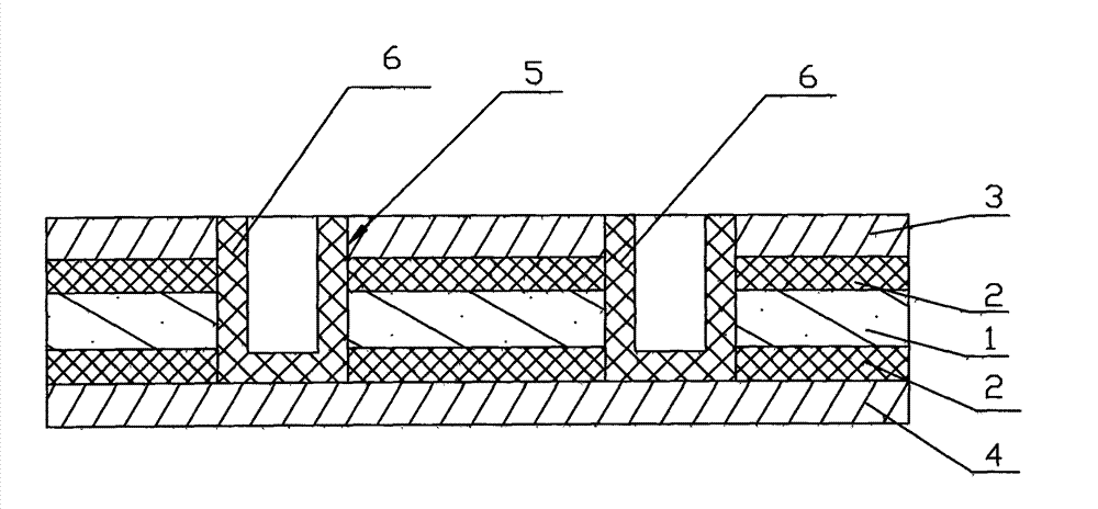
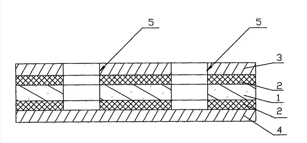
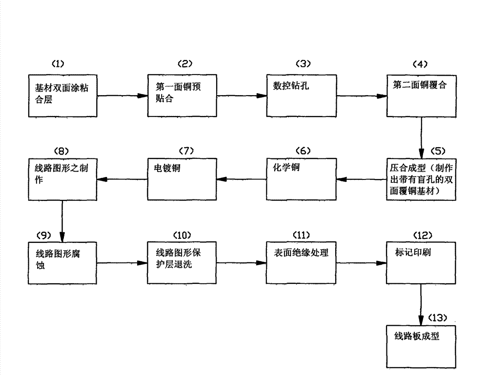
[0027] Such as Figure 1 ~ Figure 2 As shown, a double-sided circuit board with blind vias of the present invention comprises a base material layer 1 and upper and lower circuit layers 3 and 4 that are bonded together by an adhesive layer 2 respectively. The upper circuit layer 3 and the substrate layer 1 are provided with conduction blind holes 5 , along the walls of the conduction blind holes 5 , electroplated conduction walls 6 for conducting the upper and lower circuit layers 3 and 4 are electroplated.

[0028] The surface of the circuit layer 3 is provided with an electroplating surface layer integrally plated on one side with the electroplating conduction wall 6 , and the electroplating surface layer forms a part of the upper circuit layer 3 .

[0029] The line layer is pure copper foil or alloy copper foil, and the electroplated via wall 6 and the electroplated surface layer are correspondingly copper or alloy copper electroplated via layers.

[0030] The substrate layer...


PUM


Abstract

The invention discloses a blind-hole conduction double-sided circuit board and a processing method thereof. The blind-hole conduction double-sided circuit board comprises a substrate layer, an upper circuit layer and a lower circuit layer, wherein the upper circuit layer and the lower circuit layer are integrally adhered on the upper side and the lower side of the substrate layer via adhesive layers, conduction blind holes are arranged on the substrate layer and the upper circuit layer above the lower circuit layer, and an electroplating conduction wall conducting the upper circuit layer and the lower circuit layer are electroplated along the wall surface of the conduction blind holes. The blind-hole-conduction double-sided circuit board realizing blind hole conduction by copper electroplating via electroplating has the advantages of simple structure, fine conduction performance, environment friendliness and the like. The invention further provides a processing method of the blind-hole conduction double-sided circuit board, and by the processing method, production efficiency is improved, energy source consumption is reduced, conductive performance is improved, cost is reduced, and besides, the processing method is fine in quality guarantee coefficient, convenience in operation and the like.

Description

technical field [0001] The invention relates to a double-sided circuit board, in particular to a blind-hole conduction double-sided circuit board and a processing method thereof. Background technique [0002] Whether the traditional double-sided conduction circuit board is a flexible circuit board or a rigid circuit board, in its production process, mechanical drilling or laser drilling is generally used to drill conduction holes on the double-sided composite copper plate, and then pass through Blackening or electroless copper plating is applied to increase the copper thickness of the inner wall of the through hole to complete the conduction function. The process of this method has great environmental pollution. Traditional double-sided circuit boards that do not require copper plating and copper plating usually use conductive carbon Oil filling holes, conductive silver, copper paste filling holes and other forms complete the conduction function. However, although conductive...

Claims


Application Information

Patent Timeline
Patent Type & Authority Applications(China)
IPC IPC(8): H05K1/11H05K3/42
Inventor 吴祖
Owner 吴祖
Why Eureka
Try Eureka