2.5D multi-chip packaging structure of integrated antenna structure and manufacturing method thereof

A technology of multi-chip packaging and integrated antenna, which is applied in the connection of antenna grounding switch structure, antenna support/mounting device, antenna, etc., can solve the problems of high antenna signal requirements, poor heat dissipation performance, and difficulty in integrating heterogeneous chips. To achieve the effect of flexible assembly

Active Publication Date: 2020-01-03
SHANGHAI XIANFANG SEMICON CO LTD +1
View PDF5 Cites 4 Cited by
  • Summary
  • Abstract
  • Description
  • Claims
  • Application Information

AI Technical Summary

Problems solved by technology

[0006] Aiming at the problems existing in the introduction of the antenna into the multi-chip system-in-package structure, such as difficulty in integrating heterogeneous chips, high antenna signal requirements, and poor heat dissipation performance, according to an embodiment of the present invention, an integrated antenna structure is provided. 2.5D multi-chip packaging structure, including:

Method used


Image

  • 2.5D multi-chip packaging structure of integrated antenna structure and manufacturing method thereof
  • 2.5D multi-chip packaging structure of integrated antenna structure and manufacturing method thereof
  • 2.5D multi-chip packaging structure of integrated antenna structure and manufacturing method thereof

Examples


Embodiment Construction

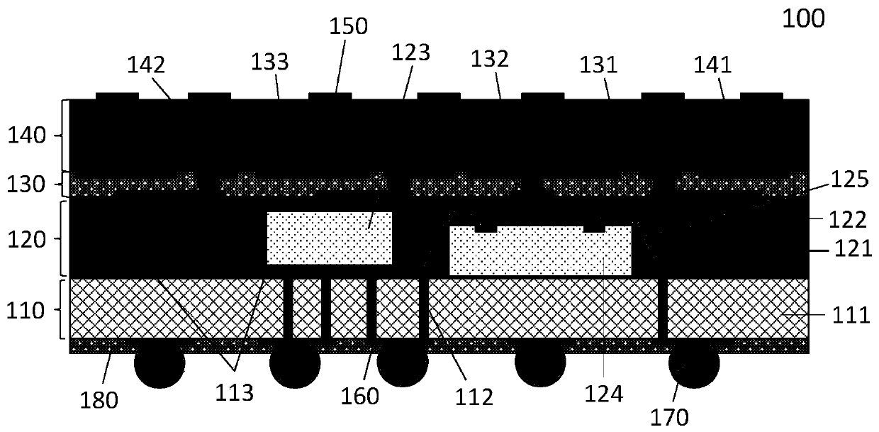
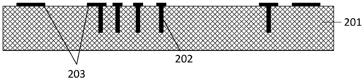
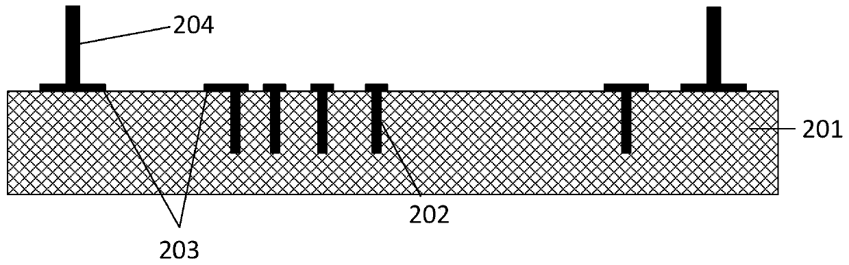
[0053] In the following description, the present invention is described with reference to various examples. One skilled in the art will recognize, however, that the various embodiments may be practiced without one or more of the specific details, or with other alternative and / or additional methods, materials, or components. In other instances, well-known structures, materials, or operations are not shown or described in detail so as not to obscure aspects of the various embodiments of the invention. Similarly, for purposes of explanation, specific quantities, materials and configurations are set forth in order to provide a thorough understanding of embodiments of the invention. However, the invention may be practiced without these specific details. Furthermore, it should be understood that the various embodiments shown in the drawings are illustrative representations and are not necessarily drawn to scale.

[0054]In this specification, reference to "one embodiment" or "the ...


PUM


Abstract

The invention discloses a 2.5D multi-chip packaging structure of an integrated antenna structure. The 2.5D multi-chip packaging structure comprises a substrate; a multi-chip plastic package layer, wherein the multi-chip plastic package layer is arranged on the substrate; a reflection interconnection layer, wherein the reflection interconnection layer is arranged on the multi-chip plastic package layer; an antenna isolation layer, wherein the antenna isolation layer is arranged on the reflection interconnection layer; the antenna array arranged on the upper surface of the antenna isolation layer; a wiring layer rearranged at the back surface of the substrate arranged at the lower portion of the substrate; an external solder balls arranged to be electrically connected with the external bonding pads of the wiring layer rearranged at the back surface of the substrate; and a passivation layer, wherein the passivation layer covers the wiring layer rearranged at the back surface of the substrate.

Description

technical field [0001] The invention relates to the technical field of semiconductor packaging, in particular to the technical fields of a 2.5D multi-chip packaging structure and a manufacturing method with an integrated antenna structure. Background technique [0002] At present, components in portable / mobile consumer electronic devices represented by mobile phones constantly require designers to provide miniaturized and low-cost product solutions. In fact, miniaturization and cost reduction are not contradictory, but complementary. [0003] With the continuous advancement of communication technology, especially the continuous development of 5G wireless communication technology, Antennas in package (AiP) has emerged. This AiP technology inherits and develops microstrip antennas, multi-chip circuit modules and tiles. Integrated concept of phased array structure. The improvement of silicon-based semiconductor process integration has driven researchers to continuously explor...

Claims


Application Information

Patent Timeline
Patent Type & Authority Applications(China)
IPC IPC(8): H01L23/66H01L23/31H01L23/367H01L23/48H01L23/552H01L25/18H01L21/98H01Q1/22H01Q1/50H01Q1/52H01Q21/00
CPCH01L23/66H01L23/3107H01L23/481H01L23/552H01L23/3677H01L25/18H01L25/50H01Q1/2283H01Q1/50H01Q1/52H01Q21/0006H01L2223/6677H01L2224/48091H01L2924/181H01L2224/48227H01L2224/16225H01L2924/00014H01L2924/00012
Inventor 戴风伟曹立强
Owner SHANGHAI XIANFANG SEMICON CO LTD
Why Eureka
Try Eureka