Communication circuit layer structure and circuit printing method thereof

A communication circuit and circuit printing technology, applied in the direction of conductive pattern formation, containing printed electrical components, etc., can solve problems such as manufacturing difficulties, achieve the effects of increased control range, accurate control, and convenient programming design

Active Publication Date: 2020-01-03
深圳市璞瑞达薄膜开关技术有限公司
View PDF6 Cites 4 Cited by
  • Summary
  • Abstract
  • Description
  • Claims
  • Application Information

AI Technical Summary

Problems solved by technology

[0004] When printing this kind of thin film circuit board, it is necessary to first judge the button position circuit and matrix arrangement state, and then arrange the combination keys, thus avoiding th

Method used


Image

  • Communication circuit layer structure and circuit printing method thereof
  • Communication circuit layer structure and circuit printing method thereof

Examples


Embodiment 1

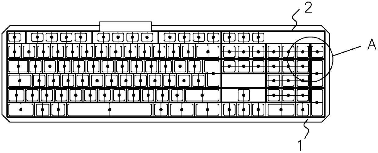
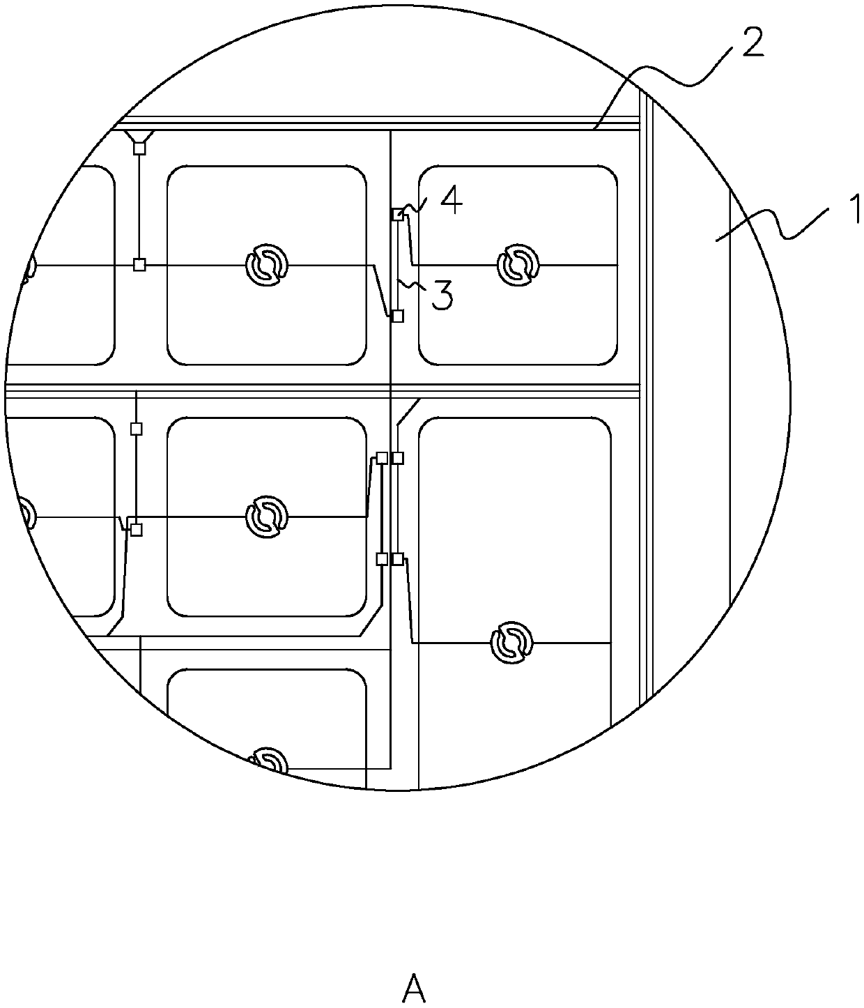
[0034] Embodiment 1: a kind of keyboard communication circuit layer structure, refer to figure 1 and figure 2 , including a flexible circuit board 1 and an insulating cover plate, the thin film circuit board is printed with a signal line 2 printed with a mixed paste, and the mixed paste is made by mixing flake-shaped particle conductive silver paste and round particle conductive silver paste. The intersection of signal lines 2 forms a multi-layer structure, and the insulation layer is formed by printing insulating ink (UV insulating ink produced by Shenzhen Zhihuadian Technology Co., Ltd., Elect-3810) between each layer to insulate and layer the intersection of signal lines 2 . Each signal line 2 is printed with an adjustment section 3 printed with electronic paste, and the adjustment section 3 selects electronic paste with different resistances according to needs.

[0035] In the case that the printing structure of the adjustment section 3 is inconvenient, when the electro...

Embodiment 2

[0037] Embodiment 2: a circuit printing method of the communication circuit layer structure in Embodiment 1, comprising the following steps:

[0038] Step 1. Prepare two plastic films, respectively the first plastic film and the second plastic film, which are respectively used to make the flexible circuit board 1 and the cover plate;

[0039] Step 2, using the electronic paste to print the signal line 2 on the first plastic film with the mixed paste, using the bridging process for multi-layer printing, and reserving the printing space for the adjustment section 3;

[0040] Step 3. According to the current design, use electronic pastes with different resistances, and print the adjustment section 3 in batches, and print the electronic pastes of each component in the same batch;

[0041] Step 4, using ultrasonic welding to connect the flexible circuit board 1 and the cover plate.

[0042] Among them, the mixed paste used in step 2 is made by mixing flake particle conductive silv...


PUM


Abstract

The invention discloses a communication circuit layer structure, which comprises a flexible circuit board, and is characterized in that a plurality of signal circuits are printed on a thin film circuit board, each signal circuit comprises an adjustment section, and the adjustment sections are printed by electronic paste with different resistance values. Through the above arrangement, the electronic paste with different resistance values is printed on each signal circuit, so that each signal circuit has an independent resistance value range, and trigger signals with different ranges are generated; the signal circuit is made of a small-resistance material, the resistance is adjusted by utilizing the electronic paste of the adjustment section, the control is accurate, and the resistance control range is expanded, so that the communication circuit can have a wider range of communication signal selection; and due to the expansion of the signal range, the same circuit structure can be applicable to more occasions, so that the situation of mutual interference of multiple combination keys is avoided during combination control among the signal circuits, and the programming design is facilitated.

Description

technical field [0001] The invention relates to the field of thin film circuit boards, in particular to a communication circuit layer structure and a circuit printing method thereof. Background technique [0002] The popularity of electronic communication products is becoming wider and wider, and it has become an indispensable existence in life, study and work, and the production and application of printed communication circuits has accelerated the development and popularization of electronic communication products. Printed communication circuits have the advantages of low cost, thinness, good flexibility, and simple design. [0003] At present, the Chinese patent with the publication number CN1247056C discloses a manufacturing method of a thin-film circuit board, which is mainly to carry out the key position circuit and matrix (Matrix) arrangement without jumping wires and avoiding the generation of unknown key signals, and then make the thin-film circuit board. When makin...

Claims


Application Information

Patent Timeline
IPC IPC(8): H05K1/16H05K3/12
CPCH05K1/16H05K3/12
Inventor 孔令海
Owner 深圳市璞瑞达薄膜开关技术有限公司
Why Eureka
Try Eureka