Microchannel positioning structure of silicon photocell and positioning method based on same

A technology of silicon photocell and positioning structure, applied in the direction of using optical devices, measuring devices, instruments, etc., can solve the problems of high demand for image processing hardware and high cost of CCD

Active Publication Date: 2020-01-10
苏州索真生物技术有限公司
View PDF5 Cites 0 Cited by
  • Summary
  • Abstract
  • Description
  • Claims
  • Application Information

AI Technical Summary

Problems solved by technology

[0003] However, the cost of the existing CCD is relatively high, and the hardware requirements for image processing are relatively high. Therefore, the present invention proposes a structure that utilizes the diffraction effect of silicon photocells and light for microchannel positioning.

Method used


Image

  • Microchannel positioning structure of silicon photocell and positioning method based on same
  • Microchannel positioning structure of silicon photocell and positioning method based on same
  • Microchannel positioning structure of silicon photocell and positioning method based on same

Examples


Embodiment 1

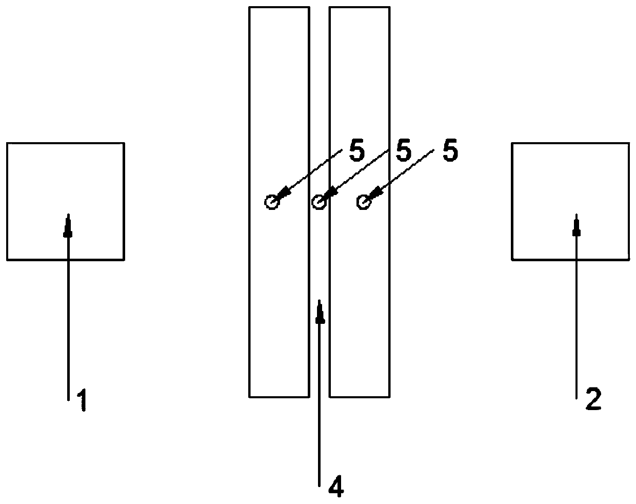
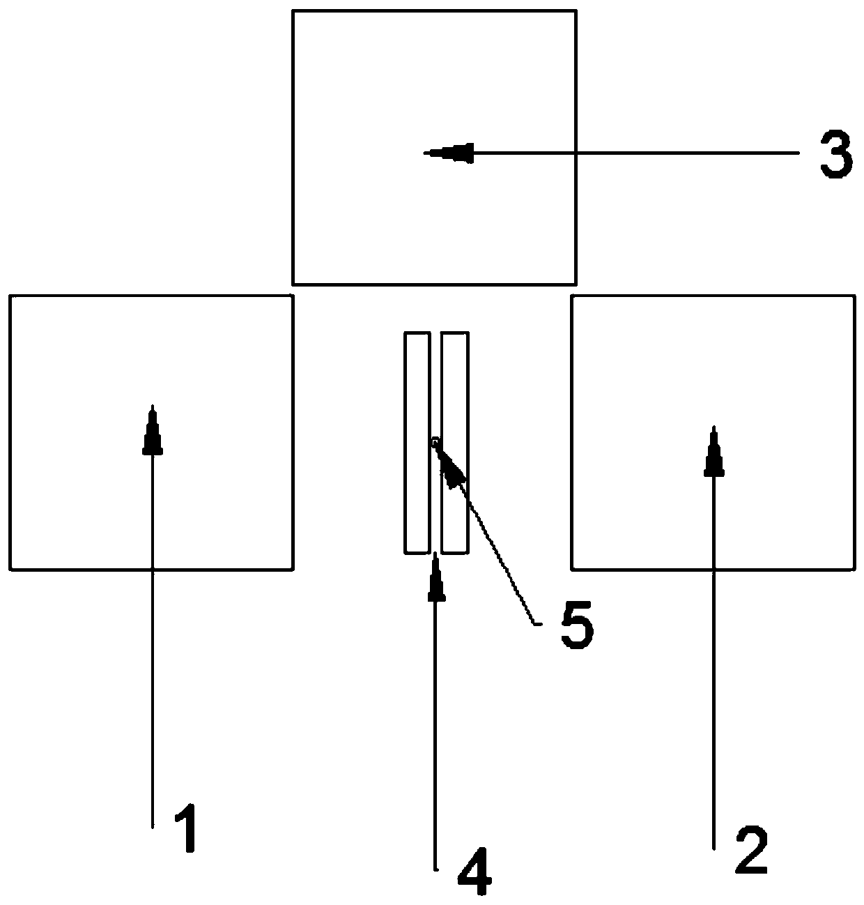
[0032] see Figure 1-9 , a microchannel positioning structure of a silicon photovoltaic cell, including a microchannel 4 and a light source 5, and also includes a silicon photovoltaic cell 6 and a mounting block 9, the bottom surface of the silicon photovoltaic cell 6 is provided with pins 7, and the silicon photovoltaic cell 6 includes a No. 1 silicon photovoltaic cell 1, No. 2 silicon photovoltaic cell 2 and No. 3 silicon photovoltaic cell 3, the installation block 9 is provided with a T-shaped installation groove 8, and No. 1 silicon photovoltaic cell 1, No. 2 silicon photovoltaic cell 2 and No. No. 1 silicon photovoltaic cell 3 is located on the perpendicular bisector of the line connecting No. 1 silicon photovoltaic cell 1 and No. 2 silicon photovoltaic cell 2. A microchannel 4 is arranged on the side of the line connecting No. 1 silicon photovoltaic cell 1 and No. 2 silicon photovoltaic cell 2, and the microchannel 4 is vertical On the plane where No. 1 silicon photovolt...

Embodiment 2

[0038] A method for positioning a microchannel positioning structure based on silicon photovoltaic cells, the steps are as follows:

[0039] 1) Install No.1 silicon photocell 1, No.2 silicon photocell 2 and No. On the vertical bisector of the photovoltaic cell 2, a microchannel 4 is arranged between the No. 1 silicon photovoltaic cell 1 and the No. One side of photocell 3;

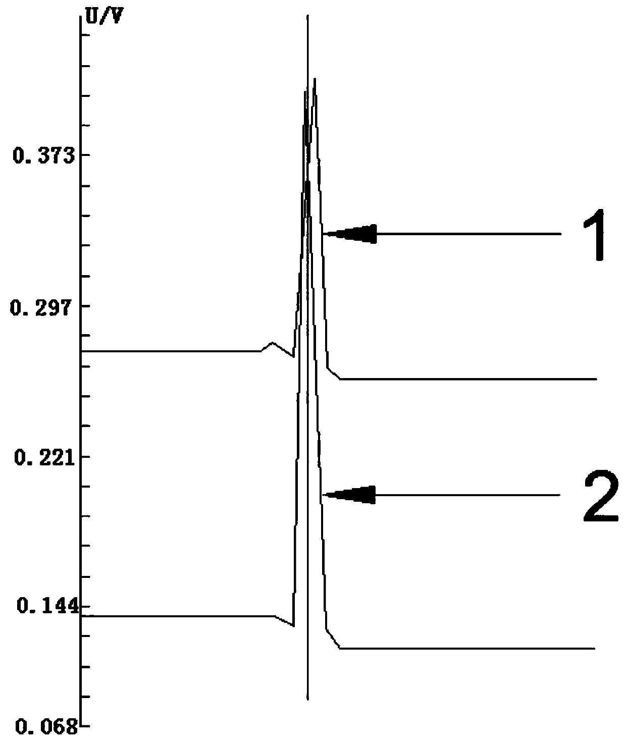
[0040] 2) The light source 5 emits light, moves the microchannel 4 vertically along the No. 1 silicon photocell 1 to the No. 2 silicon photocell 2, and detects the feedback of the photoelectric effect of the No. 1 silicon photocell 1 and No. 2 silicon photocell 2;

[0041] 3) When the light source 5 emits light through the microchannel 4, the microchannel 4 is rotated and offset along the horizontal angle. After the microchannel 4 is offset, the No. 1 silicon photovoltaic cell 1, the No. 2 silicon photovoltaic cell 2 and the Feedback of the photoelectric effect of No. 3 silicon photovoltaic cell 3;

[0...


PUM


Abstract

The present invention discloses a microchannel positioning structure of a silicon photocell. The microchannel positioning structure comprises a microchannel, a light source, a silicon photocell and aninstallation block. The silicon photocell is provided with a pin. The installation block is provided with a T-type installation groove. A first silicon photocell, a second silicon photocell and a third silicon photocell are separately installed inside the installation groove. The third silicon photocell is on a perpendicular bisector of a connection line of the first silicon photocell and the second silicon photocell. A microchannel is disposed on a side of the connection line of the first silicon photocell and the second silicon photocell. The microchannel is perpendicular to a plane of thefirst silicon photocell, the second silicon photocell and the third silicon photocell. The light source is disposed on a side of the microchannel far away from the plane of the first silicon photocell, the second silicon photocell and the third silicon photocell. Costs of microchannel positioning technologies are reduced, requirements on hardware configuration are lowered, and whether a light spotcenter is at the center of the microchannel and whether the microchannel rotates in a vertical plane can be determined by judging feedback values of only two silicon photocells.

Description

technical field [0001] The invention relates to the field of microchannel positioning, in particular to a microchannel positioning structure of a silicon photovoltaic cell and a positioning method based on the structure. Background technique [0002] A microchannel is a slit or channel with a diameter less than 20um. The existing microchannel positioning technology uses CCD image processing and positioning. The image processing and positioning technology uses a high-definition industrial camera CCD to take pictures and compare them with the calibration images. Orientation of the microchannels is performed. [0003] However, the cost of the existing CCD is relatively high, and the hardware requirements for image processing are relatively high. Therefore, the present invention proposes a structure that utilizes the diffraction effect of silicon photocells and light for microchannel positioning. Contents of the invention [0004] The purpose of the present invention is to pr...

Claims


Application Information

Patent Timeline
Patent Type & Authority Applications(China)
IPC IPC(8): G01B11/00G01B11/26
CPCG01B11/00G01B11/26
Inventor 陈谦张路李展刘泓
Owner 苏州索真生物技术有限公司
Why Eureka
Try Eureka