Super-doped silicon thin film solar cell and manufacturing method thereof

A technology of solar cells and manufacturing methods, applied in the field of solar cells, can solve the problems of large series resistance of photovoltaic devices, low photoelectric conversion efficiency, high light absorption rate of materials, etc., to meet the diffusion length limit, reduce sheet resistance and defect recombination, Reduce the effects of scattering and compounding

Active Publication Date: 2021-08-13
SICHUAN SHUWANG TECH
View PDF11 Cites 0 Cited by
  • Summary
  • Abstract
  • Description
  • Claims
  • Application Information

AI Technical Summary

Problems solved by technology

For example, the energy of light (light with a wavelength of 1.1 to 2.5 μm) that accounts for 22% of the solar energy in the near-infrared band has not been applied; the interaction between microstructure and doping causes the material to exhibit high light absorption and low The problem of photoelectric conversion efficiency; the problem of large series resistance of photovoltaic devices, limited doping depth, and low photoelectric conversion rate

Method used


Image

  • Super-doped silicon thin film solar cell and manufacturing method thereof
  • Super-doped silicon thin film solar cell and manufacturing method thereof
  • Super-doped silicon thin film solar cell and manufacturing method thereof

Examples


example 1

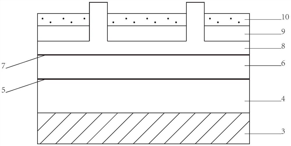
[0039] Such as figure 2 As shown, the structure of a crystalline silicon solar cell includes a P-type layer 4, a PN junction 5, an N-type layer 6, a back electrode 3 connected to the P-type layer, a light-trapping layer 7, a front electrode 8 connected to the N-type layer, and SiN x Layer 9.

[0040] The processing of crystalline silicon solar cells using the manufacturing method of the present invention is as follows.

[0041] will be like figure 1 The crystalline silicon solar cell shown as a substrate is cleaned and dried, and then an electrode mask is applied to the front electrode.

[0042] Put the crystalline silicon solar cell after the electrode mask into the vacuum chamber of the vacuum coating machine.

[0043] Vacuumize the vacuum chamber, and at the same time use graphite crucible to hold silicon particles with a purity greater than 99.9999% into the electron beam coating device, and use a tungsten boat to hold 0.001mol~0.01mol of transition metal element powde...

example 2

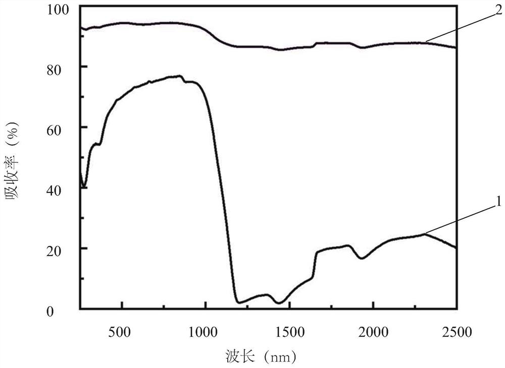
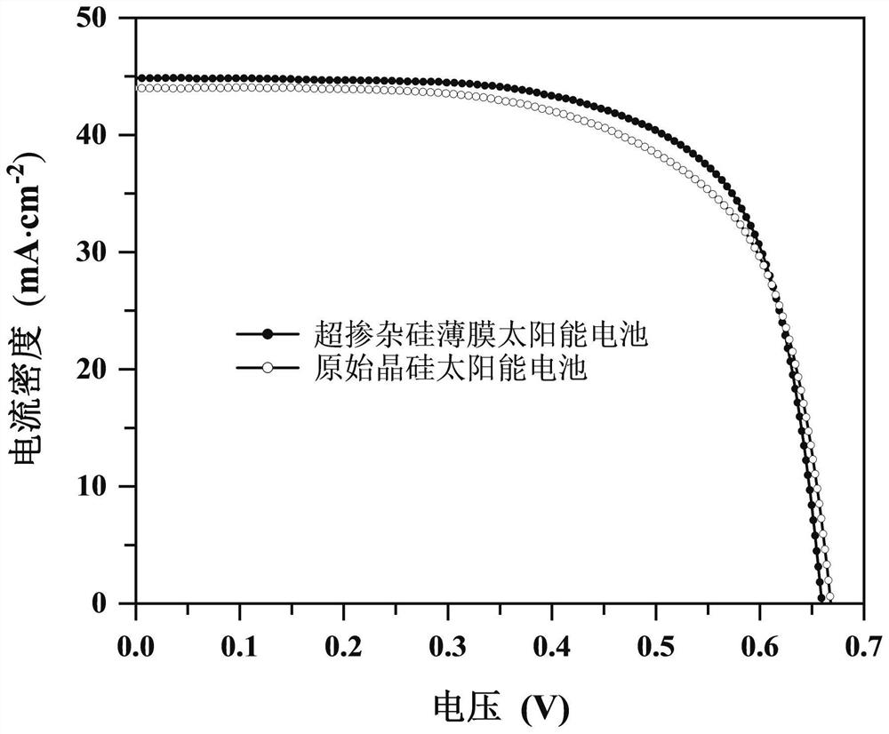
[0048] Using crystalline silicon solar cells as substrates, super-doped silicon thin-film solar cells manufactured according to the manufacturing method of the present invention. Under the same conditions, test the volt-ampere characteristics (that is, the relationship between current density and voltage) of pristine crystalline silicon solar cells and hyper-doped silicon thin-film solar cells, where the current density is in mA cm -2 , the voltage is in V, and the test results are as follows image 3 As shown, according to the test results, it can be seen that the current density (also can be said to be the absorption rate or photoelectric responsivity to light) of the super-doped silicon thin film solar cell is higher than that of the original crystalline silicon solar cell at a voltage of 0-0.6V. significantly improved.

[0049] In summary, the beneficial effects of the present invention may include:

[0050] (1) It can improve the energy utilization of the light (light w...


PUM

PropertyMeasurementUnit
thicknessaaaaaaaaaa
diameteraaaaaaaaaa

Abstract

The invention provides a super-doped silicon thin film solar cell and a manufacturing method thereof, and relates to the technical field of solar cells. The manufacturing method comprises the steps: performing electrode masking: performing electrode masking on a silicon-based solar cell serving as a substrate, and then putting the silicon-based solar cell into a vacuum chamber of a vacuum film plating machine; vacuumizing: vacuumizing the vacuum chamber; film plating: evaporating silicon particles and transition metal powder or particles to form a mixed film with the thickness of 0.05-1 [mu]m on the substrate; and doping: after the substrate is cooled, taking out the substrate, putting the substrate into a protective atmosphere, and melting the mixed film by using high-repetition-frequency nanosecond laser to form an equal-interval strip-shaped semiconductor doped layer. The invention also provides the super-doped silicon thin film solar cell which is prepared by using the method. The manufacturing method has the beneficial effects that: the solar cell capable of generating a photoelectric effect on a full spectrum can be manufactured; and transition metal is used as doped impurities to carry out silicon super-doping, and the photoelectric conversion efficiency is improved.

Description

technical field [0001] The invention relates to the technical field of solar cells, in particular to a solar cell capable of generating photoelectric effects on a full spectrum (0.25-2.5 μm) and a manufacturing method thereof. Background technique [0002] A solar cell is a thin sheet of optoelectronic semiconductor that uses sunlight to generate electricity directly. As long as it is irradiated by light that meets certain illumination conditions, it can output voltage instantly and generate current under the condition of a loop. However, limited by the band gap of silicon, the maximum wavelength for photoelectric effect is 1.12 μm. As a result, the energy of light (light with a wavelength of 1.1 to 2.5 μm) accounting for 22% of the energy of sunlight in the near-infrared band is not used. Therefore, research on photovoltaic materials and devices in the near-infrared band of the solar spectrum has been widely valued by various countries. [0003] In the prior art, there i...

Claims


Application Information

Patent Timeline
Patent Type & Authority Applications(China)
IPC IPC(8): H01L31/18H01L31/068
CPCH01L31/1804H01L31/068Y02P70/50
Inventor 温才陈凯陈青刘德雄杨永佳李同彩李晓红唐金龙石中奇
Owner SICHUAN SHUWANG TECH
Why Eureka
Try Eureka