Lithium niobate optical modulator, preparation and encapsulating method thereof
An optical modulator and packaging method technology, which is applied in the directions of light guides, optics, instruments, etc., can solve the problems of simple packaging process, complex preparation process, large size of lithium niobate waveguide chips, etc., so as to save the processing process, simplify the process, enhance the The effect of the photoelectric effect
- Summary
- Abstract
- Description
- Claims
- Application Information
AI Technical Summary
Problems solved by technology
Method used
Image
Examples
Embodiment 1
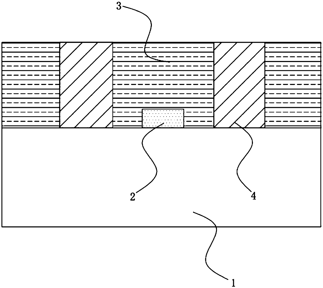
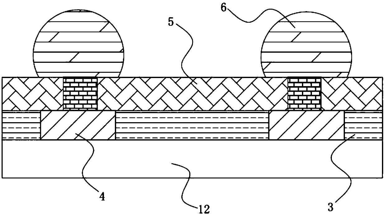
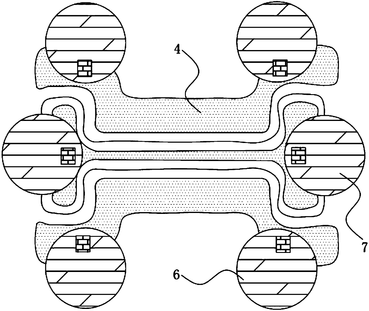
[0043] The lithium niobate optical modulator described in this embodiment will be described in detail below with reference to the accompanying drawings. Such as figure 1 , figure 2 and image 3 As shown, the lithium niobate optical modulator described in this embodiment includes a waveguide chip, a protective material 5 coated on the upper end of the waveguide chip, and a waveguide 7 connected to an external optical fiber; the waveguide chip includes a lithium niobate substrate 1, and an amorphous silicon layer 2, a silicon dioxide layer 3, and a metal electrode 4 sequentially arranged on the lithium niobate substrate 1; wherein, the thickness of the amorphous silicon layer 2 is smaller than that of the lithium niobate substrate 1 thickness, the lithium niobate substrate 1 and the amorphous silicon layer 2 together form a waveguide 12; an electrode filling area is formed on the silicon dioxide layer 3, and the metal electrode 4 is arranged in the electrode filling area ; T...
Embodiment 2
[0051] A preparation method of a lithium niobate optical modulator described in this embodiment, such as Figure 5 shown, including the following steps:
[0052] S1: Depositing a layer of amorphous silicon material on the surface of the lithium niobate substrate 1 to form an amorphous silicon layer 2, the thickness of the amorphous silicon layer 2 is smaller than the thickness of the lithium niobate substrate 1;
[0053] S2: performing photolithography development and etching stripping on the amorphous silicon layer 2 to form a waveguide 12;
[0054] S3: depositing a layer of silicon dioxide on the waveguide 12 to form a silicon dioxide layer 3;
[0055] S4: Etching on the silicon dioxide layer 3 to obtain electrode filling regions;
[0056] S5: filling the electrode filling area with metal to form the metal electrode 4 .
[0057] In this embodiment, amorphous silicon is selected as the high refractive index material to form the waveguide 12 on the lithium niobate substrate...
Embodiment 3
[0072] This embodiment is based on the packaging method of a lithium niobate optical modulator described in Embodiment 1, comprising the following steps:
[0073] Coating a protective material 5 on the waveguide chip;
[0074] setting a protective structure 6 on the outer surface of the protective material 5 on the metal electrode 4;
[0075] An insulating material is wrapped on the waveguide 7 .
PUM
| Property | Measurement | Unit |
|---|---|---|
| Thickness | aaaaa | aaaaa |
| Thickness | aaaaa | aaaaa |
| Thickness | aaaaa | aaaaa |
Abstract
Description
Claims
Application Information


