Lithium niobate photomodulator and manufacturing and packaging method thereof

A technology of optical modulator and packaging method, which is applied in the direction of light guide, optics, instrument, etc., can solve the problems of complex preparation process and large size of lithium niobate waveguide chip, and achieve the effects of simplifying the process, enhancing the photoelectric effect, and optimizing the optical loss

Active Publication Date: 2015-03-25
SUZHOU JUZHEN PHOTOELECTRIC
View PDF9 Cites 6 Cited by
  • Summary
  • Abstract
  • Description
  • Claims
  • Application Information

AI Technical Summary

Problems solved by technology

[0006] For this reason, the technical problem to be solved by the present invention is that the size of the lithium niobate waveguide chip in the prior art is relatively large, the preparation process is relatively complicated, and the packaging process is relative

Method used


Image

  • Lithium niobate photomodulator and manufacturing and packaging method thereof
  • Lithium niobate photomodulator and manufacturing and packaging method thereof
  • Lithium niobate photomodulator and manufacturing and packaging method thereof

Examples


Example Embodiment

[0043] Example 1

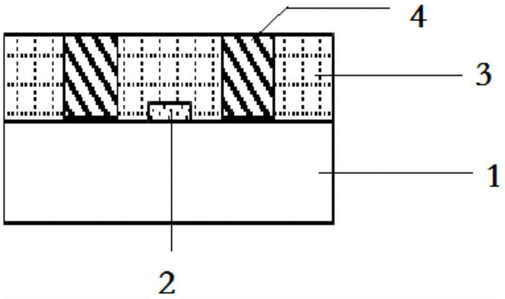
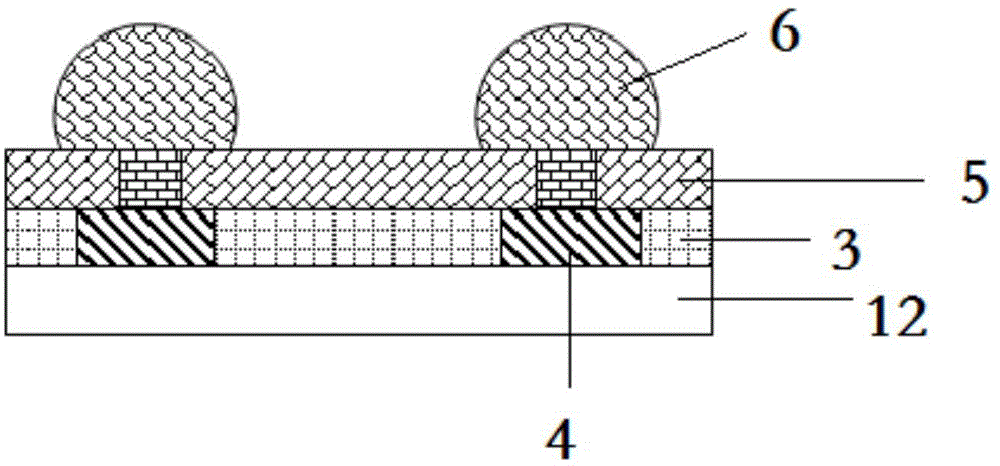
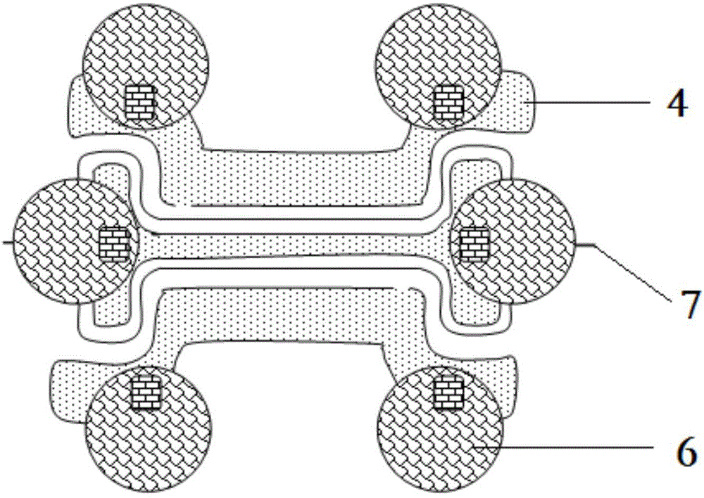
[0044] The lithium niobate optical modulator described in this embodiment will be described in detail below with reference to the accompanying drawings. like figure 1 , figure 2 and image 3 As shown, the lithium niobate optical modulator described in this embodiment includes a waveguide chip, a protective material 5 coated on the upper end of the waveguide chip, and a waveguide 7 connected to an external optical fiber; the waveguide chip includes a lithium niobate substrate 1, and an amorphous silicon layer 2, a silicon dioxide layer 3, and a metal electrode 4 sequentially arranged on the lithium niobate substrate 1; wherein, the thickness of the amorphous silicon layer 2 is smaller than that of the lithium niobate substrate 1 thickness, the lithium niobate substrate 1 and the amorphous silicon layer 2 together form a waveguide 12; an electrode filling area is formed on the silicon dioxide layer 3, and the metal electrode 4 is arranged in the electrod...

Example Embodiment

[0051] Example 2

[0052] A preparation method of a lithium niobate optical modulator described in this embodiment, such as Figure 5 shown, including the following steps:

[0053] S1: Depositing a layer of amorphous silicon material on the surface of the lithium niobate substrate to form an amorphous silicon layer, the thickness of the amorphous silicon layer being smaller than the thickness of the lithium niobate substrate;

[0054] S2: performing photolithography development and etching stripping on the amorphous silicon layer to form a waveguide;

[0055] S3: Depositing a layer of silicon dioxide on the waveguide to form a silicon dioxide layer;

[0056] S4: Etching on the silicon dioxide layer to obtain electrode filling regions;

[0057] S5: filling the electrode filling area with metal to form a metal electrode.

[0058] In this embodiment, amorphous silicon is selected as a high refractive index material to form a waveguide formed on a lithium niobate substrate. ...

Example Embodiment

[0072] Example 3

[0073] This embodiment is based on the packaging method of a lithium niobate optical modulator described in Embodiment 1, comprising the following steps:

[0074] coating a protective material on the waveguide chip;

[0075] providing a protective structure on the outer surface of the protective material on the metal electrode;

[0076] Wrap insulating material on the waveguide.


PUM

PropertyMeasurementUnit
Thicknessaaaaaaaaaa
Thicknessaaaaaaaaaa
Thicknessaaaaaaaaaa

Abstract

Provided are a lithium niobate photomodulator and a manufacturing and packaging method thereof. A waveguide structure is manufactured on a lithium niobate substrate through hydrogenated amorphous silicon, the size of a waveguide can be effectively reduced by means of the high refractive index of the amorphous silicon, and therefore the distance between metal electrodes on the lithium niobate photomodulator is reduced, and voltage needing modulating is low. A waveguide chip is preferentially manufactured by the hydrogenated amorphous silicon, and Si:H chains of the amorphous silicon can reduce optical losses. Due to the fact that the thickness of the hydrogenated amorphous silicon is adjusted, the photoelectric effect of the lithium niobate photomodulator can be maximized under the premise that the size of the waveguide is guaranteed. Due to that fact that the thickness of silicon dioxide and the thicknesses of the metal electrodes are controlled, good radio frequency matching can be guaranteed, and an optical fiber interface connected with the outside is achieved through waveguide lines penetrating through a waveguide layer; because all the waveguide lines are located in the waveguide layer, enough metal regions for packaging or testing can be reserved. The perfect packaging process can reduce the occurrence probability of the phenomenon of electric leakage, and the phenomenon that a humid environment leads to a short-circuit phenomenon is avoided.

Description

technical field [0001] The invention relates to the field of optical fiber communication transmission and communication, in particular to a lithium niobate optical modulator and a preparation and packaging method thereof. Background technique [0002] The main function of the optical modulator is to convert meaningless continuous light waves into high-frequency optical signals carrying effective information. Due to the high photoelectric effect of lithium niobate materials, lithium niobate optical modulators have become the most widely used optical modulators in existing systems. The main component of a lithium niobate optical modulator is a lithium niobate waveguide chip, and a lithium niobate optical modulator can be obtained by performing a certain packaging process on the lithium niobate waveguide chip. [0003] The existing lithium niobate waveguide chips are mainly prepared by titanium doping, etc., but due to the low contrast of the refractive index, the waveguide si...

Claims


Application Information

Patent Timeline
IPC IPC(8): G02F1/035G02B6/132
CPCG02B6/132G02F1/0316G02F1/035
Inventor 朱忻王子昊沈雷其他发明人请求不公开姓名
Owner SUZHOU JUZHEN PHOTOELECTRIC
Why Eureka
Try Eureka