Multi-layer integrated circuit layout polygon alignment and simplification processing method and device

A technology of integrated circuits and processing methods, which is applied in image data processing, 3D modeling, instruments, etc., and can solve the problem of polygon overlapping on both sides of the gap, circuit short circuit of integrated circuit layout, multi-layer integrated circuit analysis and solution time and memory. increase, etc.

Active Publication Date: 2020-01-10
北京智芯仿真科技有限公司
View PDF7 Cites 15 Cited by
  • Summary
  • Abstract
  • Description
  • Claims
  • Application Information

AI Technical Summary

Problems solved by technology

[0004] However, the inventor found in the process of implementing the present invention that the alignment and simplification of multiple polygons in the layout of multi-layer integrated circuits in the prior art only simplifies single-layer polygons, and unprocessed multi-layer polygons form a parallel flat field field Afterwards, the problem of fragmentation appeared, resulting in dense grids near the fragments when the grids of these fields were subdivided, which increased the solution time and memory of the multilayer integrated cir...

Method used


Image

  • Multi-layer integrated circuit layout polygon alignment and simplification processing method and device
  • Multi-layer integrated circuit layout polygon alignment and simplification processing method and device
  • Multi-layer integrated circuit layout polygon alignment and simplification processing method and device

Examples


Embodiment approach

[0139] As a possible implementation manner, the fourth processing module mainly includes:

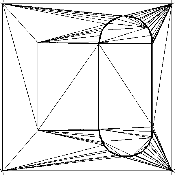
[0140] A first processing subunit, configured to align the first triangular mesh to each side of the inner and outer auxiliary polygons according to the edge exchange method to form a second triangular mesh;

[0141] The second processing subunit is used to identify the vertices of all polygons in the area clamped by the inner and outer auxiliary polygons, and define the identified vertices as being compatible with the polygon P The polygon vertices whose distance is less than a predetermined threshold;

[0142] The third processing subunit is used for each polygon, according to the identified vertices, to find the continuous identified vertices located in the polygon where the identified vertices are located, and the continuous identified vertices form a partial polygon segment or a complete polygon, is treated as the polygon P Coincident, merge the coincident partial polygon segment...


PUM


Abstract

The embodiment of the invention discloses a multi-layer integrated circuit layout polygon alignment and simplification processing method and device. The method comprises the following steps of projecting a plurality of polygons of a multilayer integrated circuit layout to a same layer, and forming a Delaunay triangular mesh according to a Delaunay triangulation algorithm; aligning the Delaunay triangular mesh to each edge of each polygon, calculating the intersection points of the edges of each polygon, and adding the intersection points into the polygon vertexes and the Delaunay triangular mesh nodes to form a first triangular mesh; on the basis, forming the inner and outer auxiliary polygons for clamping the polygons inside and outside each polygon, and controlling the distances betweenthe inner and outer auxiliary polygons and the polygons through the distance thresholds; and aligning and simplifying the edges of each layer of polygons falling between the inner and outer auxiliarypolygons. According to the present invention, the fragmentation problem after the multilayer polygons form the parallel flat plate field domain can be reduced, the unnecessary dense grids are reduced,the analysis and solving time and the required memory of the multilayer integrated circuit are shortened, the gaps among the polygons can be reserved, and the integrated circuit layout shape is basically not changed.

Description

technical field [0001] The invention relates to the field of simplified processing of integrated circuit layout polygons, in particular to a multilayer integrated circuit layout polygon alignment and simplified processing method and device. Background technique [0002] The layout of the integrated circuit is the intermediate link between the schematic diagram of the integrated circuit and the realization of the integrated circuit process, and it is an indispensable and important link. [0003] Since the thickness and layer spacing of the multilayer integrated circuit board are much smaller than the size of the board, the three-dimensional electromagnetic wave calculation field of the multilayer integrated circuit board can be simplified into multiple two-dimensional calculation fields, and the two-dimensional calculation field is the upper and lower The parallel plate field of layer coupling is also the propagation area of ​​electromagnetic waves. The parallel plate field ...

Claims


Application Information

Patent Timeline
IPC IPC(8): G06T17/20
CPCG06T17/205
Inventor 唐章宏
Owner 北京智芯仿真科技有限公司
Why Eureka
Try Eureka