Display panel, manufacturing method thereof and display device

A display panel and manufacturing method technology, which is applied in semiconductor/solid-state device manufacturing, semiconductor devices, electrical components, etc., can solve problems such as abnormal display of the display panel with binding patterns, and achieve the effect of avoiding short circuit of binding patterns and avoiding abnormal display

Active Publication Date: 2020-01-10
BOE TECH GRP CO LTD +1
View PDF3 Cites 6 Cited by
  • Summary
  • Abstract
  • Description
  • Claims
  • Application Information

AI Technical Summary

Problems solved by technology

[0005] In order to solve the problems of the related technology, the embodiment of the present invention provides a display panel and its manufacturing method, and

Method used


Image

  • Display panel, manufacturing method thereof and display device
  • Display panel, manufacturing method thereof and display device
  • Display panel, manufacturing method thereof and display device

Examples


Embodiment Construction

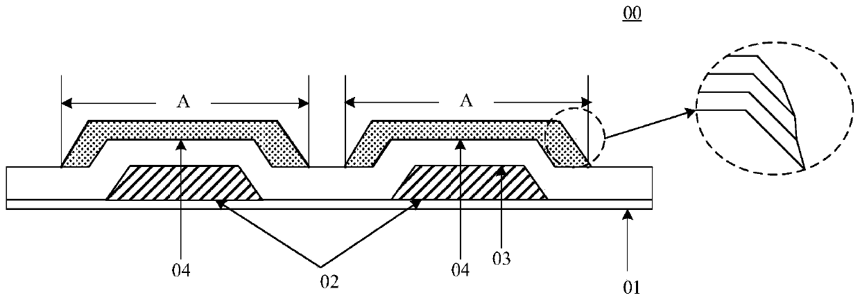
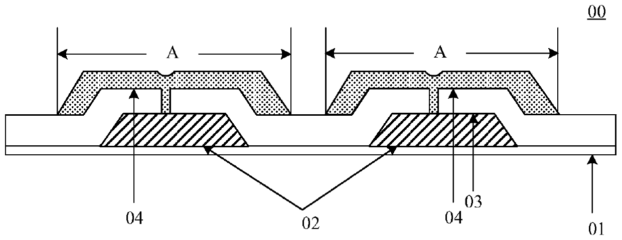
[0051] In order to make the object, technical solution and advantages of the present invention clearer, the implementation manner of the present invention will be further described in detail below in conjunction with the accompanying drawings.

[0052] In the related art, multiple layers of metal materials are often used to form the bonding pattern. When the anode layer is etched with an etchant, the interlayer of the multiple layers of metal materials exposed on the side of the bond pattern will undergo a displacement reaction with the etchant.

[0053]For example, the multilayer metal material is a titanium / aluminum / titanium (i.e. Ti / Al / Ti) material, that is, the multilayer metal material is a three-layer metal material, the metal material of the middle interlayer is aluminum, and the upper and lower layers of the middle interlayer Both layers of metal materials are titanium; the anode to be etched can also be made of multilayer material, for example, the multilayer material ...


PUM

PropertyMeasurementUnit
Thicknessaaaaaaaaaa

Abstract

The invention discloses a display panel, a manufacturing method thereof and a display device, and belongs to the technical field of display. The method comprises the steps: forming a binding pattern comprising at least one conducting layer on a substrate, wherein the surface, away from the substrate, of each conducting layer has a binding area; forming a flat layer on the substrate on which the binding pattern is formed, and processing the flat layer into a flat layer pattern, wherein the flat layer pattern comprises an opening area and a shielding area, the orthographic projection of the binding area on the substrate being located in the orthographic projection of the opening area on the substrate, and the orthographic projection of the side surface of the conducting layer on the substrate being located in the orthographic projection of the shielding area on the substrate. In this way, the shielding area can cover the area, where an interlayer is possibly exposed, of the side surfaceof the conducting layer, so that replacement reaction between anode etching liquid and metal material of the interlayer is avoided, the risk of short circuit caused by the fact that replaced metal isattached to the binding pattern is also avoided, and the abnormal display phenomenon of the display panel is also avoided.

Description

technical field [0001] The present invention relates to the field of display technology, in particular to a display panel, a manufacturing method thereof, and a display device. Background technique [0002] Chip on film (COF) is a packaging technology for fixing a driver integrated circuit on a flexible circuit board, and has been widely used in the field of display technology. The COF can be used to connect the printed circuit board and the display panel, and is used to transmit the data signal received from the printed circuit board to the display panel, so as to drive the display panel for display. [0003] Wherein, the COF connects the printed circuit board and the display panel through the binding pattern provided thereon. In the related art, in order to simplify the manufacturing process of the display panel, the binding pattern on the COF is arranged on the same layer as the source-drain metal pattern of each pixel in the display area. In order to form an anode on t...

Claims


Application Information

Patent Timeline
IPC IPC(8): H01L21/77H01L27/12
CPCH01L27/1259H01L27/1244H01L27/1248H01L27/124H01L24/02H01L24/05H01L27/1288H01L2224/0221H01L2224/05073H01L2224/05553H01L2224/05559H01L2224/05573
Inventor 杨中流
Owner BOE TECH GRP CO LTD
Why Eureka
Try Eureka