Semiconductor device
A semiconductor and non-conduction technology, applied in the fields of semiconductor devices and power conversion devices, to achieve the effects of low conduction loss, improved trade-off relationship, and improved controllability
- Summary
- Abstract
- Description
- Claims
- Application Information
AI Technical Summary
Problems solved by technology
Method used
Image

Examples
Embodiment 1
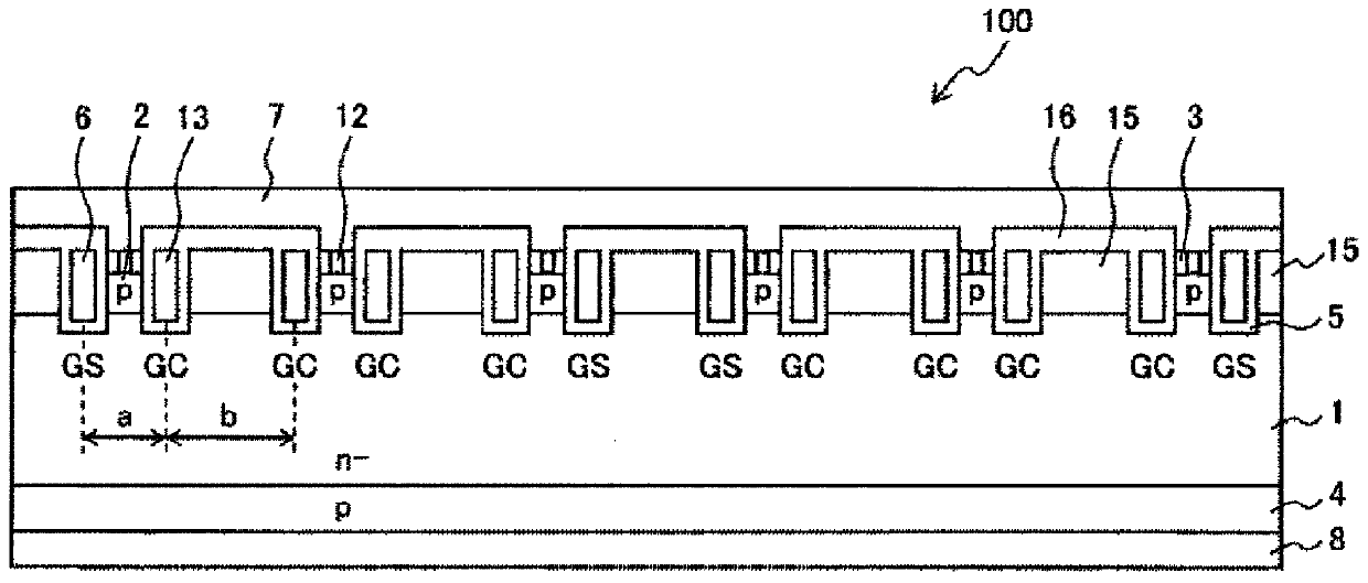
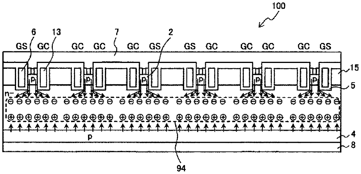
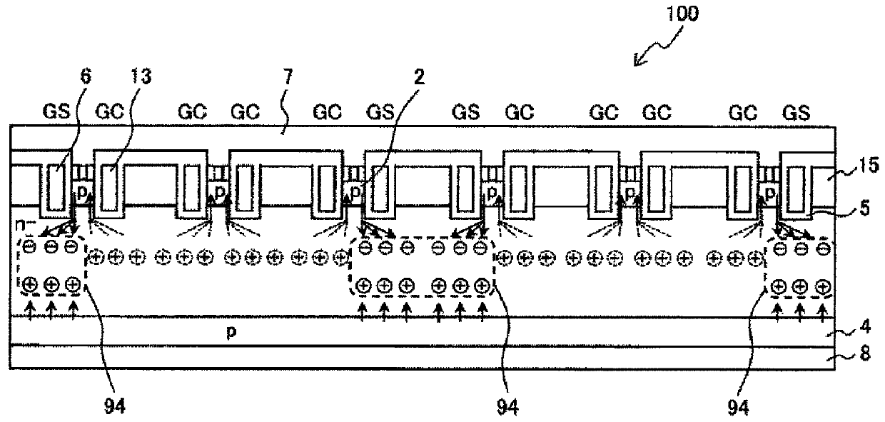
[0050] refer to Figure 1 to Figure 5 Next, an insulated gate type (gate control type) semiconductor device (IGBT) 100 according to the first embodiment of the present invention will be described. figure 1 It is a partial sectional view of IGBT100 of this Example.
[0051] This example figure 1 As shown, an IGBT having a trench gate shape and two independently controllable gates (GS, GC) has a p-type well layer 2 adjacent to the n-type drift layer 1 in the vertical direction, and The side opposite to the p-type well layer 2 is the p-type collector layer 4 adjacent to the n-type drift layer 1 in the longitudinal direction. Furthermore, on the upper part of the p-type well layer 2, the p-type power supply layer 12 and the n-type emitter layer 3 are adjacently present. Furthermore, these p-type well layer 2 and n-type emitter layer 3 are connected to a trench gate type first insulating gate (GS gate) 6 having a gate electrode and a gate insulating film (gate oxide film) 5 vi...
Embodiment 2
[0067] refer to Figure 6A as well as Figure 6B Next, an insulated gate type (gate control type) semiconductor device (IGBT) 200 according to a second embodiment of the present invention will be described. Figure 6A is a partial sectional view of the IGBT of this embodiment, and additionally Figure 6B is a plane configuration diagram of the IGBT of this embodiment, Figure 6B The section of the A-A' part in the Figure 6A corresponding to the sectional view.
[0068] This embodiment is an IGBT having a trench gate shape and having two independently controllable gates, and includes a p-type well layer 2 adjacent to the n-type drift layer 1 in the vertical direction, and a p-type well layer 2 adjacent to the p-type drift layer 2 The opposite side is the p-type collector layer 4 adjacent to the n-type drift layer 1 in the longitudinal direction. Furthermore, on the upper part of the p-type well layer 2, the p-type power supply layer 12 and the n-type emitter layer 3 are a...
Embodiment 3
[0076] refer to Figure 8 to Figure 9B Next, an insulated gate type (gate control type) semiconductor device (IGBT) 300 according to a third embodiment of the present invention will be described. Figure 8 It is a sectional view of IGBT300 of this Example.
[0077] This embodiment relates to a side gate shape in which the gate electrode is arranged only on the sidewall of the trench, and is an IGBT having two independently controllable gates. A p-type well layer 2 vertically adjacent to the n-type drift layer 1 is provided, and a p-type collector layer 4 vertically adjacent to the n-type drift layer 1 on the side opposite to the p-type well layer 2 . Furthermore, on the upper part of the p-type well layer 2, the p-type power supply layer 12 and the n-type emitter layer 3 are adjacently present. Furthermore, these p-type well layer 2 and n-type emitter layer 3 are connected to a side-gate-type first insulating gate (GS gate) 6 having a gate electrode and a side gate through ...
PUM
 Abstract
Description
Claims
Application Information
 - R&D Engineer
- R&D Manager
- IP Professional
- Industry Leading Data Capabilities
- Powerful AI technology
- Patent DNA Extraction
Browse by: Latest US Patents, China's latest patents, Technical Efficacy Thesaurus, Application Domain, Technology Topic.
© 2024 PatSnap. All rights reserved.Legal|Privacy policy|Modern Slavery Act Transparency Statement|Sitemap