Display device

A display device and display panel technology, which is applied in computer monitor shells, instruments, electrical digital data processing, etc., can solve problems such as stress dispersion, screen damage, panel deformation, etc., and achieve increased resistance, smooth buffer layer, and slow down local damage Effect

Inactive Publication Date: 2020-01-17
WUHAN CHINA STAR OPTOELECTRONICS SEMICON DISPLAY TECH CO LTD
View PDF7 Cites 9 Cited by
  • Summary
  • Abstract
  • Description
  • Claims
  • Application Information

AI Technical Summary

Problems solved by technology

Therefore, after a point impact, usually the stress cannot be quickly dispersed, and the panel is severely deformed due to local stress concentration, causing damage to the screen
At the same time, in the current module stacking structure, the contact surface between each film layer is mostly a horizontal contact surface. Although the preparation process is simple, it is not conducive to the stress dispersion after point impact.

Method used


Image

  • Display device
  • Display device

Examples


Embodiment Construction

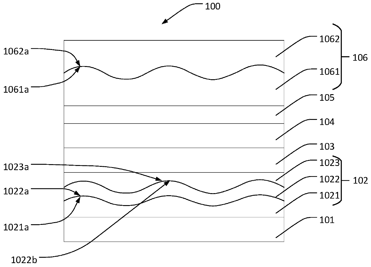
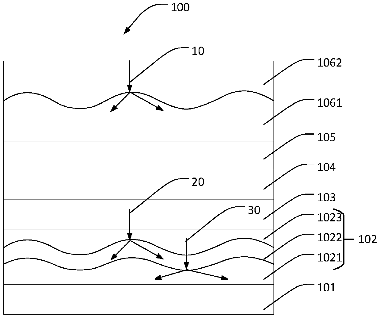
[0027] The following description of various embodiments is made with reference to the accompanying drawings to illustrate specific embodiments in which the invention may be practiced. The directional terms mentioned in the present invention, such as up, down, front, back, left, right, inside, outside, side, etc., are only directions referring to the drawings. The component names mentioned in the present invention, such as first, second, etc., are only used to distinguish different components, which can be better expressed. In the figures, structurally similar elements are denoted by the same reference numerals.

[0028] Embodiments of the present invention will be described in detail herein with reference to the accompanying drawings. This invention may be embodied in many different forms and should not be construed as only the specific embodiments set forth herein. These embodiments are provided to explain the practical application of the invention, so that others skilled i...


PUM


Abstract

According to the display device provided by the invention, the opposite surfaces of the base material and the hardened coating of a glass cover plate are arranged to be of an uneven structure, so thatthe flatness of the glass cover plate can be ensured, and stress can be diffused under point impact. Meanwhile, uneven structures are arranged on the two sides of the protective layer at the same time, stress can be diffused, the upper side and the lower side of the protective layer are flattened through the flattening layers to form the buffer layer, and the whole buffer layer is smoother. The display device provided by the invention can improve the resistance to point impact and alleviate local damage.

Description

technical field [0001] The present invention relates to the display field, in particular to a display device. Background technique [0002] In order to meet the bending characteristics of flexible organic light-emitting diode (OLED) display devices, organic film materials with better bending properties are often used as glass cover plates. In order to improve hardness, hard coatings are usually spin-coated on organic substrates. material, so as to achieve the purpose of hardening the surface layer, but its hardness is still significantly lower than that of the glass cover. Therefore, after a point impact, usually the stress cannot be dispersed quickly, and the panel is relatively seriously deformed due to local stress concentration, causing damage to the screen. At the same time, in the current module stacking structure, the contact surface between each film layer is mostly a horizontal contact surface. Although the preparation process is simple, it is not conducive to the ...

Claims


Application Information

Patent Timeline
Patent Type & Authority Applications(China)
IPC IPC(8): H01L51/52
CPCH10K50/841H10K50/84H10K50/844G06F1/1601G02B1/04G02B1/14G02B5/3025C08L67/00C08L33/24G06F1/1609C09K2323/06G02F1/133331
Inventor 王芳
Owner WUHAN CHINA STAR OPTOELECTRONICS SEMICON DISPLAY TECH CO LTD
Why Eureka
Try Eureka