A vertical LED chip structure and manufacturing method thereof

A technology of LED chips and manufacturing methods, which is applied in the direction of semiconductor devices, electrical components, circuits, etc., to achieve the effect of increasing the light output ratio

Active Publication Date: 2022-04-19
XIAMEN CHANGELIGHT CO LTD
View PDF11 Cites 0 Cited by
  • Summary
  • Abstract
  • Description
  • Claims
  • Application Information

AI Technical Summary

Problems solved by technology

[0003] However, the luminous efficiency of vertical LED chips in the prior art can be further improved.

Method used


Image

  • A vertical LED chip structure and manufacturing method thereof
  • A vertical LED chip structure and manufacturing method thereof
  • A vertical LED chip structure and manufacturing method thereof

Examples


Embodiment Construction

[0074] As mentioned in the background art section, the luminous efficiency of the vertical LED chip structure in the prior art can be further improved.

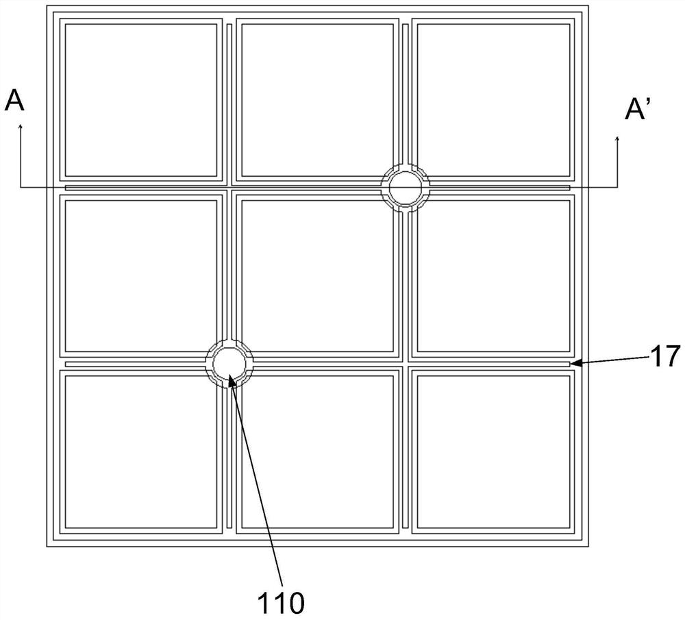
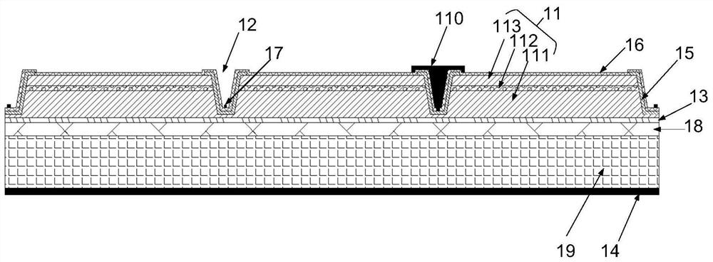
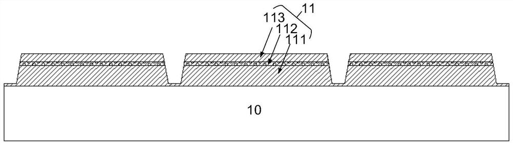
[0075] The inventors found that the reason for the above problems is that in the prior art, for high-power vertical LED chips, the chip area is usually relatively large, and the common ones are 45mil╳45mil, 60mil╳60mil, etc., but the quality of the current epitaxial materials However, defects such as threading dislocations can cause chip failure, and often a small defect can cause the failure of the entire LED chip. Therefore, the larger the area of ​​the LED chip, the lower the overall yield of the chip, but the price of the chip will also be higher. high. Moreover, due to the large refractive index difference between LED epitaxial semiconductor materials and air, the solid angle for photons emitted from multiple quantum wells (MQWs) to escape from the LED surface is very small, and a large proportion of photons are in the w...


PUM


Abstract

The application discloses a vertical LED chip structure and a manufacturing method thereof. In the vertical LED chip structure, a groove is formed on the LED epitaxial structure at least through the light-emitting layer and the second-type semiconductor layer, and the groove connects the LED The epitaxial structure is divided into multiple sub-mesas. For the front-mounted structure, the groove separating the mesas can directly increase the light output ratio of the side wall of the LED chip. For the flip-chip structure, because the side wall of the groove can emit light to the light-emitting layer Reflect the light, change the path of light emitted by the light-emitting layer, and avoid the large refractive index difference between the LED epitaxial semiconductor material and air, so that a certain proportion of light forms multiple total reflections in the semiconductor material similar to propagating in the waveguide , is finally absorbed and consumed, resulting in the problem of low luminous efficiency of the vertical LED chip structure.

Description

technical field [0001] The invention relates to the technical field of semiconductor device fabrication, in particular to a vertical LED chip structure and a fabrication method thereof. Background technique [0002] Vertical LED chips are high-performance LED chips with advantages such as high light efficiency, good heat dissipation, and high reliability. They are generally used to prepare high-power, high-brightness, and high-performance LED chips. Combined with the increasingly mature wafer bonding and epitaxial lift-off technology, the LED epitaxial layer can be transferred to the second substrate with good conductivity and heat dissipation. There are a series of problems such as poor performance and weak heat dissipation. On the other hand, the back reflector of the LED chip can not only better realize the current expansion of the bottom layer of the chip, but also greatly improve the light output efficiency of the LED. At present, vertical LED chips are often used to p...

Claims


Application Information

Patent Timeline
Patent Type & Authority Patents(China)
IPC IPC(8): H01L27/15H01L33/00H01L33/10H01L33/24
CPCH01L27/156H01L33/005H01L33/24H01L33/10
Inventor 赵斌陈凯轩曲晓东刘英策李俊贤
Owner XIAMEN CHANGELIGHT CO LTD
Why Eureka
Try Eureka