Semiconductor laser and method for manufacturing the same

a semiconductor and laser technology, applied in the field of buried heterostructure, can solve the problems of difficult process, leakage current generation, inability to prevent the substitution of doped ions, etc., and achieve the effect of improving the light output ratio

Inactive Publication Date: 2005-06-09
ELECTRONICS & TELECOMM RES INST
View PDF6 Cites 0 Cited by
  • Summary
  • Abstract
  • Description
  • Claims
  • Application Information

AI Technical Summary

Benefits of technology

[0018] The present invention is directed to a semiconductor laser capable of improving a ratio of a light output to an input current by blocking a leakage current flowing outside an active waveguide in a BH laser, and a method for manufacturing the same.

Problems solved by technology

However, in the case of growing the semi-insulating semiconductor layer, there has been a problem that Fe ion is replaced by Zn ion doped into the p type semiconductor layer, so that the semi-insulating semiconductor would be changed into the p type semiconductor.
If the thickness of the n type semiconductor layer becomes too thin, substitution of the doped ions cannot be prevented.
As described above, in the case of employing the method of etching the current blocking layer around the mesa structure and then filling the etched portions with the semi-insulating semiconductor, a characteristic of the BH laser can be enhanced, however, a leakage current may be generated if the current blocking layer does not work sufficiently at a high temperature or a high operation current.
In addition, it is difficult to perform processes since the etched depth is deep, and processes would be complicated since the semi-insulating semiconductor layer should be grown.
Further, the width of the mesa structure cannot be formed narrowly due to difficulty of a deep etching process and an inter diffusion phenomenon, in which Zn and Fe ions are substituted each other.

Method used


Image

  • Semiconductor laser and method for manufacturing the same
  • Semiconductor laser and method for manufacturing the same
  • Semiconductor laser and method for manufacturing the same

Examples


Embodiment Construction

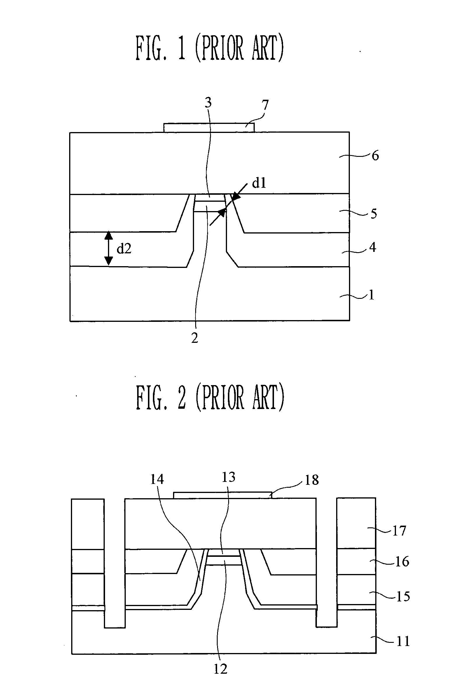
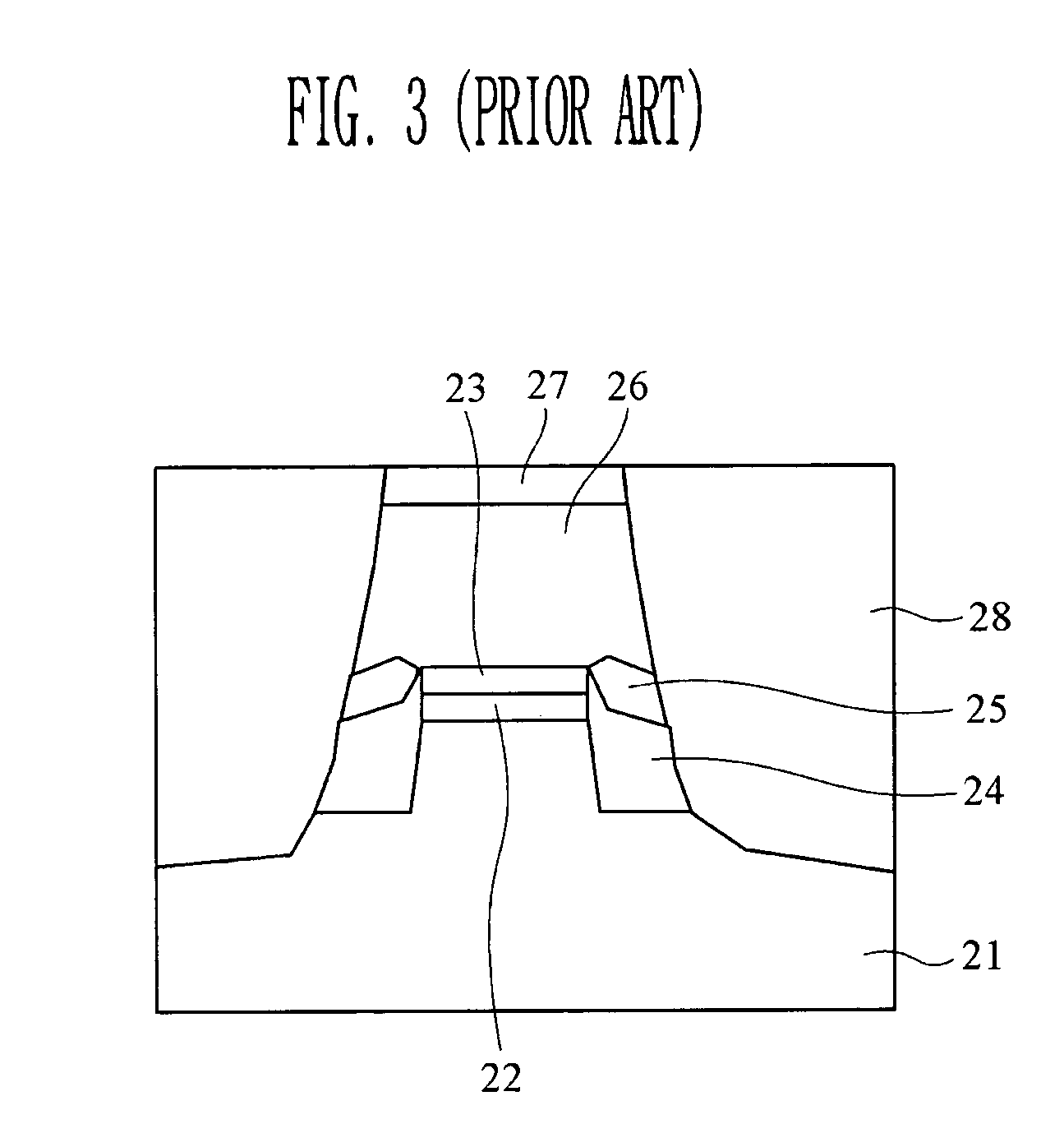
[0034] Hereinafter, the embodiments of the present invention will be explained with reference to the accompanying drawings. However, the embodiment of the present invention can be changed into a various type, and it should be not understood that the scope of the present invention is limit to the following embodiments. The embodiments of the present invention are provided in order to explain the present invention to those skilled in the art. On the other hand, like numerals present like elements throughout the several figures and the repeated explanation of the element will be omitted.

[0035]FIG. 4A is a schematic view of a current blocking layer comprising semiconductor layers. This structure may be represented by a circuit, in which a p-n-p transistor Q1 and an n-p-n transistor Q2 are connected in a pair between a power supply terminal Vac and a ground, as shown in FIG. 4B. FIG. 5 is a graph showing current-voltage characteristic of transistors Q1 and Q2 of FIG. 4B, obtained by cal...


PUM


Abstract

Provided is a semiconductor laser including a substrate etched into a mesa structure, an active layer, clad layers, a current blocking layer, an etch-stop, an ohmic contact layer, and electrodes, and a method for manufacturing the same, whereby it is possible to improve a ratio of light output to input current by blocking a leakage current flowing outside an active waveguide in a BH laser.

Description

BACKGROUND [0001] 1. Field of the Invention [0002] The present invention relates to a buried heterostructure and, more particularly, to a semiconductor laser capable of improving a ratio of light output to input current by blocking a leakage current, which flows outside an active waveguide, and a method for manufacturing the same. [0003] 2. Discussion of Related Art [0004] Generally, a buried heterostructure (BH) laser has an excellent ratio of light output to input current since currents could be injected only into an active waveguide, restrictively. For preventing currents from flowing outside the active waveguide in the BH laser, two methods for blocking currents have been used, as follow. [0005] According to one method, a thyristor is formed by alternatively stacking two semiconductor layers doped with p type and n type. [0006] For example, U.S. Pat. No. 5,665,612 (“Method for fabricating a planar buried heterostructure laser diode” by J. K. Lee et al.) proposes a method for gro...

Claims


Application Information

Patent Timeline
Patent Type & Authority Applications(United States)
IPC IPC(8): H01L21/00H01L33/00H01S5/20H01S5/223H01S5/227H01S5/32
CPCH01S5/209H01S5/223H01S2301/18H01S5/3211H01S5/3213H01S5/227
Inventor SONG, JUNG HOLEE, CHUL WOOKKIM, KI SOOBAEK, YONG SOON
Owner ELECTRONICS & TELECOMM RES INST
Why Eureka
Try Eureka