LED (light-emitting diode) module with cross-over electrode and manufacturing method thereof

A technology of light-emitting diodes and manufacturing methods, which is applied in semiconductor/solid-state device manufacturing, circuits, electrical components, etc., and can solve the problem of reduced light output efficiency from the side of light-emitting diodes 12, reduced luminous efficiency of light-emitting diodes 12, and inability to accurately control film thickness, etc. problem, achieve the effect of improving coating uniformity, avoiding expensive equipment, and reducing equipment cost

Inactive Publication Date: 2013-01-23
UBILUX OPTOELECTRONICS CORP
View PDF4 Cites 0 Cited by
  • Summary
  • Abstract
  • Description
  • Claims
  • Application Information

AI Technical Summary

Problems solved by technology

The insulating layer 13 that fills the channel 120 has a thickness of about several microns (μm), and SiO of this thickness 2 The insulating layer 13 has a transmittance of about 25% to 45% for light with a wavelength of about 455 nanometers (nm), which reduces the lateral light output efficiency of the light emitting diode 12, thereby reducing the overall luminous efficiency of the light emitting diode 12.
[0007] In addition, the insulating layer 13 must be formed by spin coating instead of vacuum coating methods such as sputtering and evaporation, because the speed of vacuum coating is relatively slow, and it will take too much time to coat a film layer with a thickness of several microns.
Although the film forming speed of the spin coating is fast, the disadvantage is that the film thickness cannot be accurately controlled, and the excessively protruding part of the insulating layer 13 needs to be polished by chemical mechanical polishing (CMP) afterwards, and the CMP equipment The cost is high, so there is a lack of high equipment cost

Method used


Image

  • LED (light-emitting diode) module with cross-over electrode and manufacturing method thereof
  • LED (light-emitting diode) module with cross-over electrode and manufacturing method thereof
  • LED (light-emitting diode) module with cross-over electrode and manufacturing method thereof

Examples


Embodiment Construction

[0027] The present invention will be described in detail below with reference to the accompanying drawings and embodiments. It should be noted that in the following description, similar elements are denoted by the same numerals.

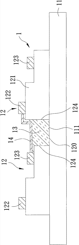
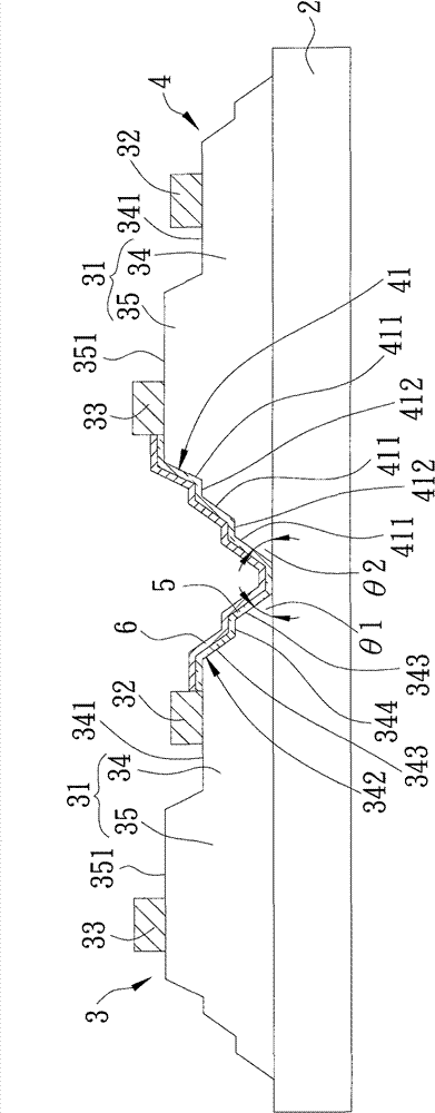
[0028] refer to image 3 , the preferred embodiment of the light-emitting diode module with jumper electrodes in the present invention is suitable for DC-driven LED modules, and is also suitable for AC-driven LED modules, and includes: a substrate 2, located on the left and right intervals A first light emitting diode 3 and a second light emitting diode 4 on the substrate 2 , an insulating layer 5 and a jumper electrode 6 .

[0029] The substrate 2 of the present embodiment is sapphire (Al 2 o 3 ) Substrate 2, but not limited thereto. The first light emitting diode 3 and the second light emitting diode 4 have the same structure, and both include a light emitting body 31, an n-electrode 32 and a p-electrode 33, and the light-emitting body 31 includ...


PUM


Abstract

The invention provides an LED (light-emitting diode) module with a cross-over electrode and a manufacturing method thereof. The LED module comprises a substrate, two LEDs, an insulating layer and the cross-over electrode, wherein the two LEDs are spaced apart on the substrate and the opposite surfaces of the two LEDs are stepped surfaces; the insulating layer is covered on the stepped surfaces, thus the insulating layer is also in a stepped thin film state; and the cross-over electrode is covered on the surface of the insulating layer and two sides of the cross-over electrode are respectivelyconnected with the n electrode of one LED and the p electrode of the other LED. In the LED module, by designing the stepped surfaces, the thinner insulating layer covers the cross-over electrode, thus increasing the emergent light proportion of the LEDs in a side direction and the overall light-emitting efficiency.

Description

technical field [0001] The invention relates to a light-emitting diode module and its manufacturing method, in particular to a light-emitting diode module with jumper electrodes and its manufacturing method. Background technique [0002] The existing light emitting diode (LED) module includes a plurality of light emitting diodes arranged in an array, and electrodes of adjacent light emitting diodes are connected by jumper electrodes, so that each light emitting diode can be electrically connected. Since the design of the jumper circuits between adjacent LEDs is the same, only two of the LEDs in the module will be described below. [0003] Such as figure 1 As shown, the two LEDs 12 on a substrate 11 of the LED module 1 both include: a light-emitting body 121 and a p-electrode 122 and an n-electrode 123 located on the surface of the light-emitting body 121 . The opposite sides 124 of the two light emitting diodes 12 and a top surface 111 of the substrate 11 jointly define a ...

Claims


Application Information

Patent Timeline
Patent Type & Authority Patents(China)
IPC IPC(8): H01L27/15H01L21/782
Inventor 林志胜郑舜鸿
Owner UBILUX OPTOELECTRONICS CORP
Why Eureka
Try Eureka