Circuit substrates, circuit boards and display assemblies

A circuit substrate and circuit board technology, applied in the directions of printed circuits, electrical components, printed circuits, etc., can solve the problems of unfavorable circuit board thickness control, unreasonable setting of electrical components, and poor experience effect, etc., to improve user experience, Realize the effect of thin design and thin thickness

Active Publication Date: 2021-09-07
OPPO CHONGQING INTELLIGENT TECH CO LTD
View PDF8 Cites 0 Cited by
  • Summary
  • Abstract
  • Description
  • Claims
  • Application Information

AI Technical Summary

Problems solved by technology

[0002] In the related art, the electrical components are arranged on the circuit substrate to be connected with the circuit substrate. Due to the unreasonable arrangement of the electrical components, the circuit board composed of the electrical components and the circuit substrate is relatively thick, which is not conducive to the control of the thickness of the entire circuit board. Poor user experience when used in display components

Method used


Image

  • Circuit substrates, circuit boards and display assemblies
  • Circuit substrates, circuit boards and display assemblies
  • Circuit substrates, circuit boards and display assemblies

Examples


Embodiment Construction

[0029] Embodiments of the present application are described in detail below, examples of which are shown in the drawings, wherein the same or similar reference numerals denote the same or similar elements or elements having the same or similar functions throughout. The embodiments described below by referring to the figures are exemplary, and are only for explaining the present application, and should not be construed as limiting the present application.

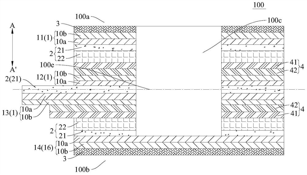
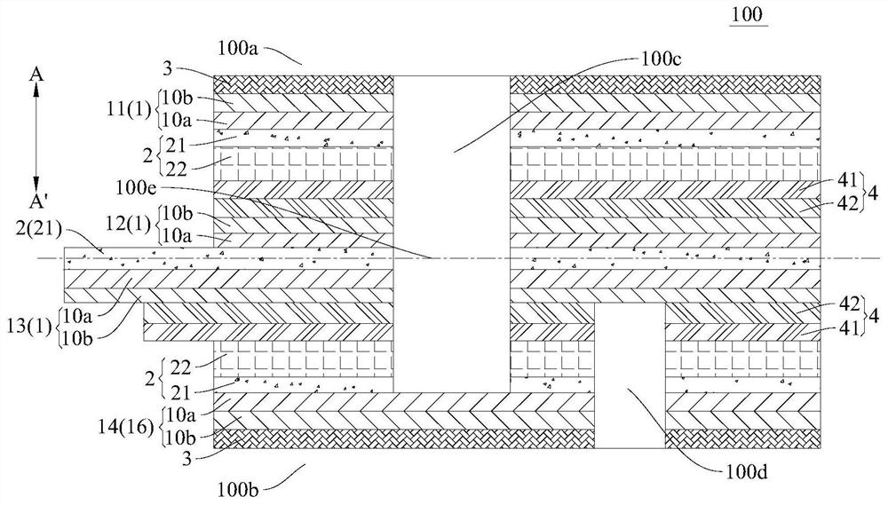
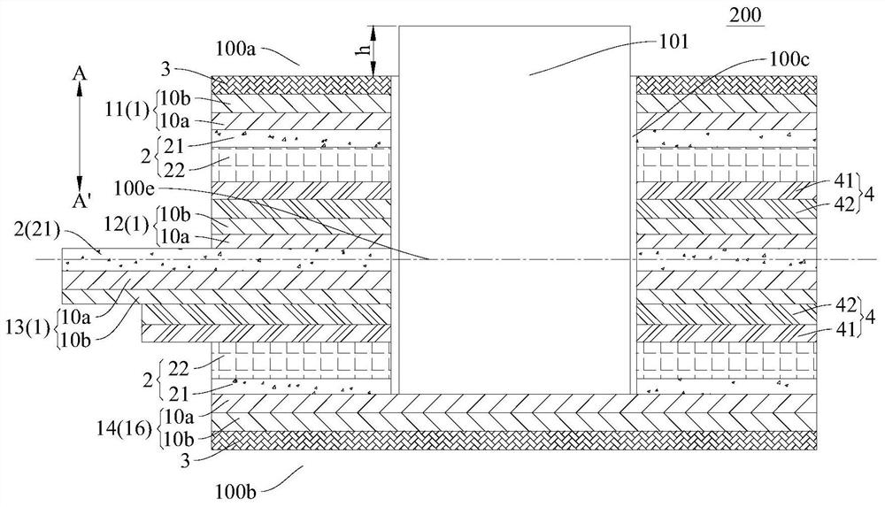
[0030] Refer below Figure 1-Figure 3 A circuit substrate 100 according to an embodiment of the present application is described.

[0031] like Figure 1-Figure 3 As shown, according to the circuit substrate 100 of the embodiment of the present application, the circuit substrate 100 is suitable for disposing the circuit element 101, and the circuit element 101 is suitable for being electrically connected with the circuit substrate 100, and the two sides of the thickness of the circuit substrate 100 are respectively the firs...


PUM


Abstract

The present application discloses a circuit substrate, which is suitable for setting circuit elements. The two sides of the thickness of the circuit substrate are respectively the first side and the second side. A first blind hole, the circuit substrate includes n wiring layers, the n wiring layers are stacked, and an insulating layer is provided between two adjacent wiring layers to separate the wiring layers on adjacent sides, Along the direction from the first side to the second side, the first layer of the multi-layer wiring layer is the first wiring layer, the last layer of the multi-layer wiring layer is the nth wiring layer, and the first blind hole penetrates at least the first wiring layer. A wiring layer, which penetrates to the (1+m)th wiring layer, and the circuit element installed in the first blind hole is connected to the (1+m)th wiring layer, wherein, m is a positive integer, and n is greater than 1 positive integer, and m<n. According to the circuit substrate of the present application, the structure is simple, which is conducive to reducing the thickness of the circuit board and realizing the thinning design of the circuit board.

Description

technical field [0001] The present application relates to the field of display technology, in particular to a circuit substrate, a circuit board and a display screen assembly. Background technique [0002] In the related art, the electrical components are arranged on the circuit substrate to be connected with the circuit substrate. Due to the unreasonable arrangement of the electrical components, the circuit board composed of the electrical components and the circuit substrate is relatively thick, which is not conducive to the control of the thickness of the entire circuit board. When used in display components, the user experience is poor. Contents of the invention [0003] This application aims to solve at least one of the technical problems existing in the prior art. To this end, the present application proposes a circuit substrate, which has a simple structure and is conducive to reducing the thickness of the circuit board and realizing the thinning design of the circ...

Claims


Application Information

Patent Timeline
Patent Type & Authority Patents(China)
IPC IPC(8): H05K1/18G09F9/00
CPCG09F9/00H05K1/183H05K2201/09518
Inventor 贾玉虎
Owner OPPO CHONGQING INTELLIGENT TECH CO LTD
Why Eureka
Try Eureka