Power MOS device and manufacturing method thereof

A technology of MOS devices and manufacturing methods, which is applied to semiconductor devices, electrical components, circuits, etc., can solve problems such as hindering device performance, affecting device reliability, and large on-resistance of power MOS devices, so as to improve device reliability and reduce On-resistance, the effect of improving the overall performance

Inactive Publication Date: 2020-01-31
SEMICON MFG ELECTRONICS (SHAOXING) CORP
View PDF0 Cites 0 Cited by
  • Summary
  • Abstract
  • Description
  • Claims
  • Application Information

AI Technical Summary

Problems solved by technology

However, excessive thinning of the semiconductor substrate will affect the reliability of the device. Usually, it is necessary to reserve a substrate thickness of at least 60 microns, which makes the resistance of the semiconductor substrate still occupy a large proportion in the composition of the on-resistance. And the on-resistance of the power MOS device is still relatively large, which hinders the improvement of the performance of the device

Method used


Image

  • Power MOS device and manufacturing method thereof
  • Power MOS device and manufacturing method thereof
  • Power MOS device and manufacturing method thereof

Examples


Embodiment Construction

[0029] The power MOS device and its manufacturing method of the present invention will be further described in detail below with reference to the drawings and specific embodiments. The advantages and features of the present invention will become clearer from the following description. It should be noted that in the following description, many specific details and numerical values ​​are given in order to provide a more thorough understanding of the present invention. However, it is obvious to those skilled in the art that the present invention may not require one or more In other instances, some technical features known in the art are not described in order to avoid obscuring the present invention. It should be understood that the drawings in the description are all in very simplified form and use imprecise scales, and are only used to facilitate and clearly assist the purpose of illustrating the embodiments of the present invention.

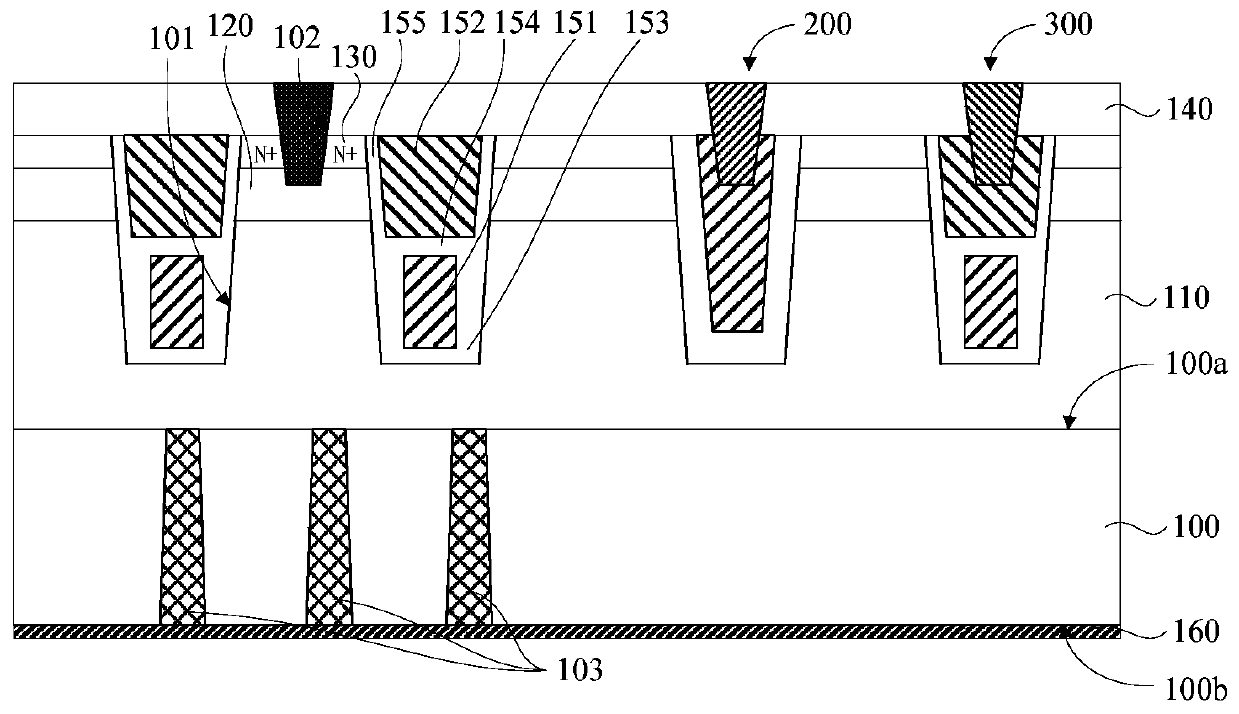
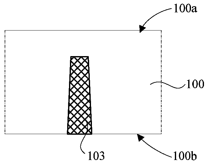
[0030] The power MOS devices in the embod...


PUM


Abstract

The invention relates to a power MOS device and a manufacturing method thereof. The power MOS device comprises a semiconductor substrate. The first surface of the semiconductor substrate is provided with an epitaxial layer. The epitaxial layer includes a drift region and a well region and a source region located on the drift region. The second surface of the semiconductor substrate is provided with a drain metal layer, wherein a conductive plug is arranged in the semiconductor substrate and the resistivity of the conductive plug is less than that of the surrounding semiconductor substrate. Theconductive plug is arranged so that the effect of reducing the on-resistance can be achieved without excessively thinning the semiconductor substrate and the on-resistance of the power MOS device canbe reduced and the reliability of the device can also be improved.

Description

technical field [0001] The invention relates to the technical field of semiconductors, in particular to a power MOS device and a manufacturing method thereof. Background technique [0002] Compared with ordinary MOS devices, power MOS devices add a low-doped drift region, allowing part of the voltage to fall on the drift region, which can improve the ability of the device to resist traditional channel breakdown, gate oxide layer breakdown, and junction breakdown , so it has better high pressure resistance and is widely used in medium and high pressure fields. [0003] An ideal power MOS device should have a lower on-resistance and a higher breakdown voltage, wherein the on-resistance is not only related to the drift region, but also related to the resistance of the semiconductor substrate. When the existing power MOS device is manufactured, it will The semiconductor substrate is thinned to reduce resistance, and the thinned semiconductor substrate is used as the drain regio...

Claims


Application Information

Patent Timeline
Patent Type & Authority Applications(China)
IPC IPC(8): H01L29/06H01L29/78
CPCH01L29/0603H01L29/0615H01L29/0684H01L29/78
Inventor 宋金星谢志平
Owner SEMICON MFG ELECTRONICS (SHAOXING) CORP
Why Eureka
Try Eureka