Resistive random access memory and preparation method thereof

A resistive memory, resistive technology, used in electrical components and other directions

Pending Publication Date: 2020-01-31
SHANGHAI HUALI MICROELECTRONICS CORP
View PDF15 Cites 1 Cited by
  • Summary
  • Abstract
  • Description
  • Claims
  • Application Information

AI Technical Summary

Problems solved by technology

The structure of a common resistive variable memory: a substrate, a lower electrode (TiN) located on the substrate, a resistive material layer (TaOx) located on the lower electrode and the upper surface of the substrate, and a resistive material layer (TaOx) located on the upper surface of the resistive The upper electrode (TiN) above the variable material layer, this kind of resistive memory can generally only realize dual-value storage in high and low resistance states

Method used


Image

  • Resistive random access memory and preparation method thereof
  • Resistive random access memory and preparation method thereof
  • Resistive random access memory and preparation method thereof

Examples


Embodiment Construction

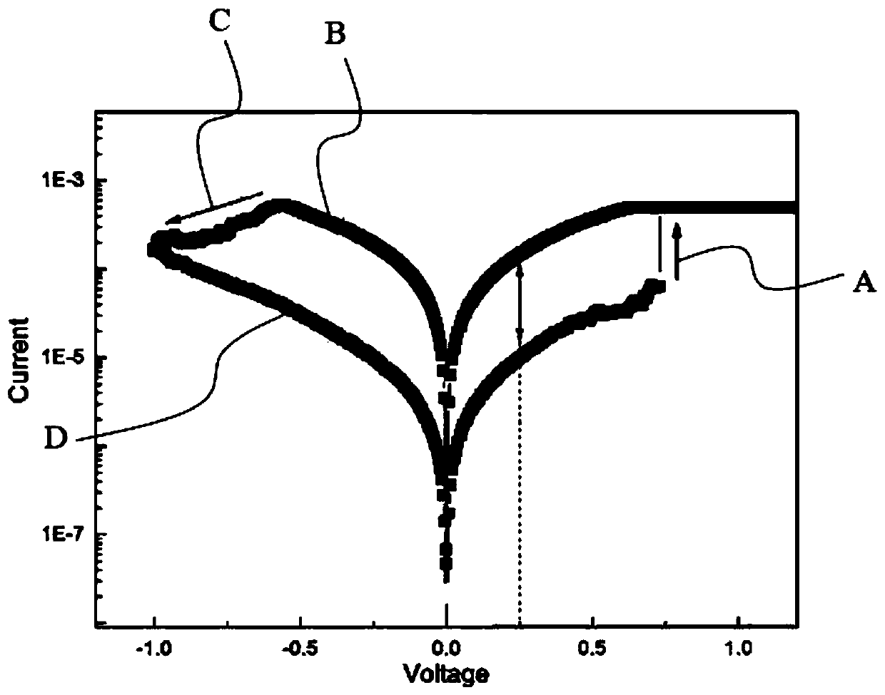
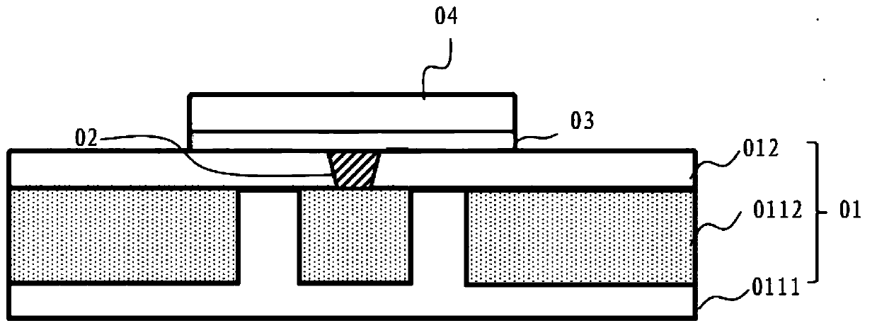
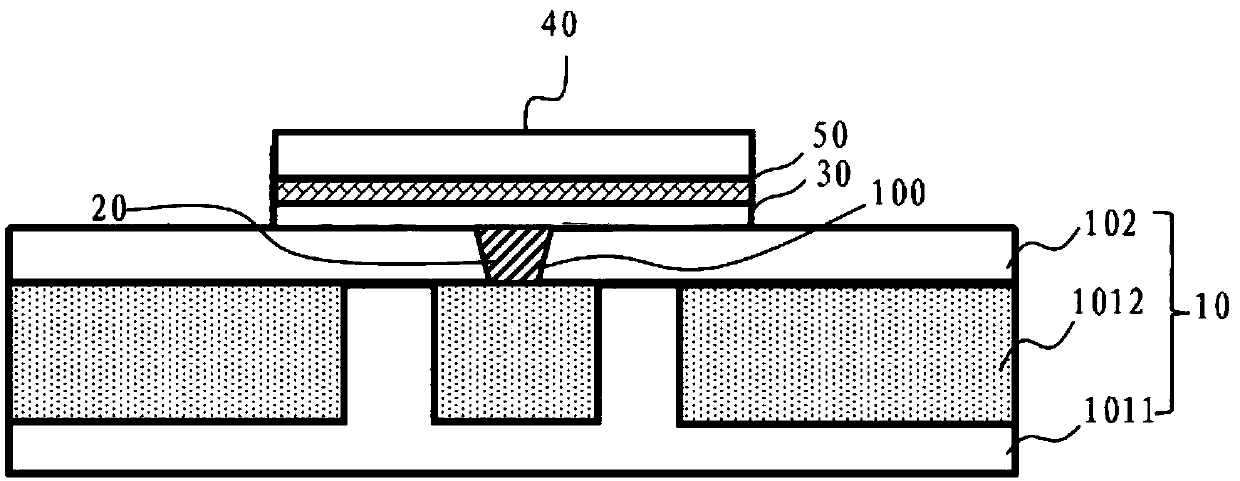
[0031] With the rapid development of modern information technology, people's demand for non-volatile memory with faster speed, higher capacity and lower power consumption is increasing. As a research hotspot of next-generation memory, resistive memory has strong application potential and is considered to be the memory with the most commercial value. The working principle of the resistive variable memory is that the resistive material realizes high-low resistance state transition under electric drive, thereby realizing data storage. like figure 1 It is the high-low resistance transition I-V curve of common resistive memory, A is the transition from high resistance state to low resistance state, B is the low resistance state, C is the transition from low resistance state to high resistance state, and D is the high resistance state. The common resistive memory structure is to grow a layer of resistive material between the upper and lower electrodes. This kind of resistive memory...


PUM


Abstract

The invention provides a preparation method of a resistive random access memory. The preparation method comprises the following steps: providing a substrate; forming a lower electrode on the substrate; forming a first resistive random material layer on the lower electrode and the upper surface of the substrate; forming a second resistive random material layer on the first resistive random materiallayer, wherein the resistive state of the second resistive random material layer is different from that of the first resistive random material layer; and forming an upper electrode on the second resistive random material layer. The second resistive random material layer is additionally arranged between the first resistive random material layer and the upper electrode so that the conversion undervarious resistance states (>2) of the resistive random access memory can be realized, and thus multi-value memory can be realized and the data storage amount can be increased on the premise that the memory chip area is unchanged.

Description

technical field [0001] The invention relates to the field of semiconductors, in particular to a resistive variable memory and a preparation method thereof. Background technique [0002] With the rapid development of modern information technology, people are constantly pursuing non-volatile memory chips with faster speed, higher capacity and lower power consumption to store massive data. The widespread use of smart phones and tablet computers and the promotion of cloud computing have put forward higher requirements on the performance and capacity of non-volatile memory chips. The current development trend of embedded non-volatile memory is large capacity, low power consumption, high density, high speed and low cost. [0003] With the further shrinking of the logic process, especially after entering the 40nm process node, it is more difficult to integrate traditional EEPROM or NORFLASH with the advanced logic process represented by HKMG and FinFET, and its high manufacturing ...

Claims


Application Information

Patent Timeline
Patent Type & Authority Applications(China)
IPC IPC(8): H01L45/00
CPCH10N70/00H10N70/046H10N70/011
Inventor 邹荣陈昊瑜王奇伟
Owner SHANGHAI HUALI MICROELECTRONICS CORP
Why Eureka
Try Eureka