A gaas pHEMT 2/3 dual-mode frequency division circuit
A circuit and mode division technology, applied in the field of GaAspHEMT2/3 dual-mode frequency division circuit, can solve the problems such as the inability to meet the requirements of ultra-high frequency circuits and the narrow operating frequency range of the circuit
- Summary
- Abstract
- Description
- Claims
- Application Information
AI Technical Summary
Problems solved by technology
Method used
Image
Examples
Embodiment 1
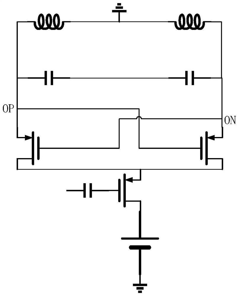
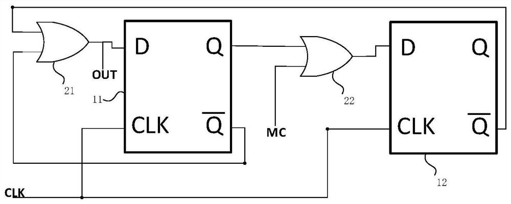
[0074] See figure 2 , figure 2 It is a schematic structural diagram of a GaAs pHEMT 2 / 3 dual-mode frequency division circuit provided by an embodiment of the present invention, including:
[0075] A frequency divider core circuit 1, connected to the logic gate circuit 2, for receiving a high-frequency differential signal, and outputting a level signal after frequency-dividing the high-frequency differential signal;
[0076] A logic gate circuit 2, connected to the frequency divider core circuit 1, for outputting a dual-mode frequency division signal after performing logic operations on the level signal;
[0077] Wherein, both the frequency divider core circuit 1 and the logic gate circuit 2 include a level conversion circuit.
[0078] See image 3 ,See figure 2 , figure 2 It is another structural schematic diagram of the GaAs pHEMT 2 / 3 dual-mode frequency division circuit provided by the embodiment of the present invention,
[0079] In this embodiment, the frequency ...
Embodiment 2
[0134] The effects of the present invention will be further described through simulation experiments below.
[0135] In this embodiment, the circuit diagram of the simulation experiment can be found in Figure 5 , including frequency divider core circuit, logic gate circuit, differential input sinusoidal signal CLK, CLKN and external DC bias voltage MC, MCN; differential input sinusoidal signal CLK, CLKN is connected to frequency divider core circuit, external DC bias voltage MC and MCN are connected to the logic gate circuit, and the differential output signal is connected to the output of the logic gate circuit. Using transient simulation, the amplitude of the two clock signals is 1V, the frequency is 6GHz, and the phase is 0° and 180°. MC and MCN are -1V, or -2V, V1=-1V, V2=-3V.
[0136] See Figure 7a~7b , Figure 7a~7b is the simulation result diagram provided by the embodiment of the present invention, where Figure 7a MC=-1V, MCN=-2V, at this time, the circuit reali...
PUM
 Abstract
Description
Claims
Application Information


