

Process for producing a structured metal layer on a substrate body, and substrate body having a structured metal layer
a technology of structured metal and substrate body, which is applied in the direction of conductive pattern formation, transportation and packaging, chemical instruments and processes, etc., can solve the problems of insufficient thickness between metal foil and substrate body, insufficient structure metal foil, and high electrical resistance of pastes, etc., to achieve simple and time-saving effects
- Summary
- Abstract
- Description
- Claims
- Application Information
AI Technical Summary
Benefits of technology
Problems solved by technology
Method used
Image

Examples
Embodiment Construction
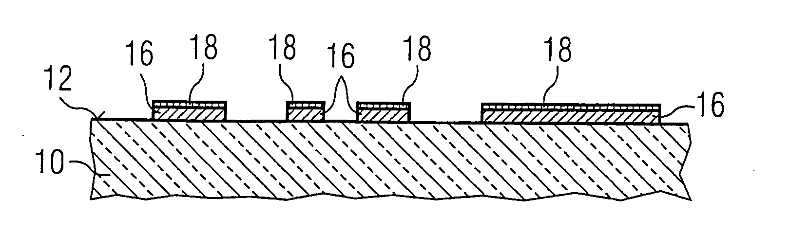
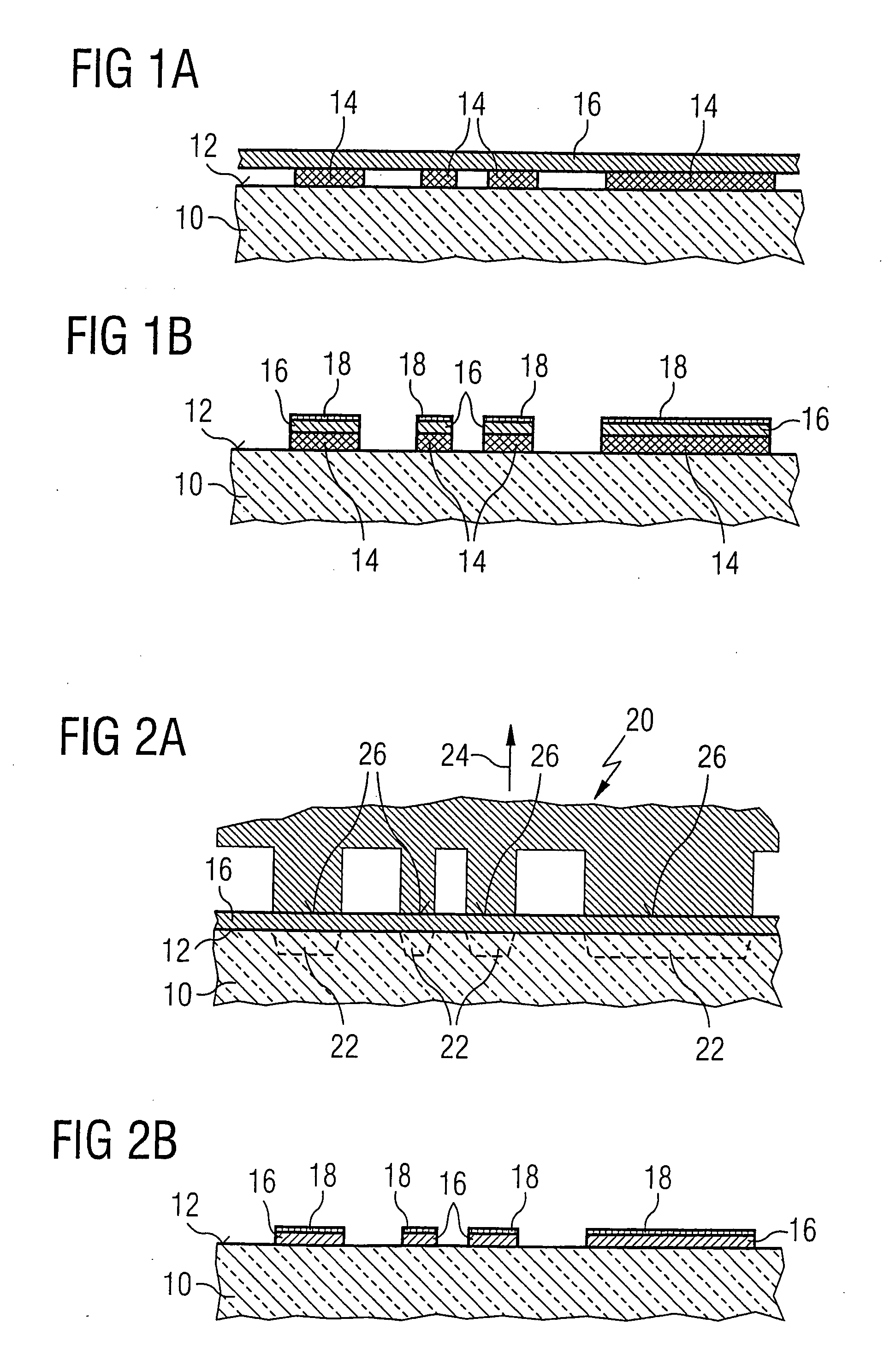
[0038]FIG. 1A illustrates, in excerpt and sectional form, a substrate body 10, to the surface 12 of which, in a first process step, an at least partially structured bonding layer 14, for example comprising an adhesive, resist or the like, has been applied. The substrate body 10 may consist, for example, of plastic, metal, ceramic, glass or any other desired material. Then, a metal foil 16 is applied to the entire surface of the substrate body 10 which has been provided with the structured bonding layer 14. The metal foil 16 is fixed to the surface 12 of the substrate body 10 with the aid of the structured bonding layer 14.
[0039] After the metal foil 16 has been fixed, those regions of the metal foil 16 which are not joined to the bonding layer—i.e. which lie laterally next to the structured layer of adhesive 14—are mechanically removed from the substrate body 10, which can be effected, for example, by brushing them off. The configuration of the substrate body following this step is...
PUM
| Property | Measurement | Unit |
|---|---|---|
| Thickness | aaaaa | aaaaa |
| Melting point | aaaaa | aaaaa |
Abstract
Description
Claims
Application Information