

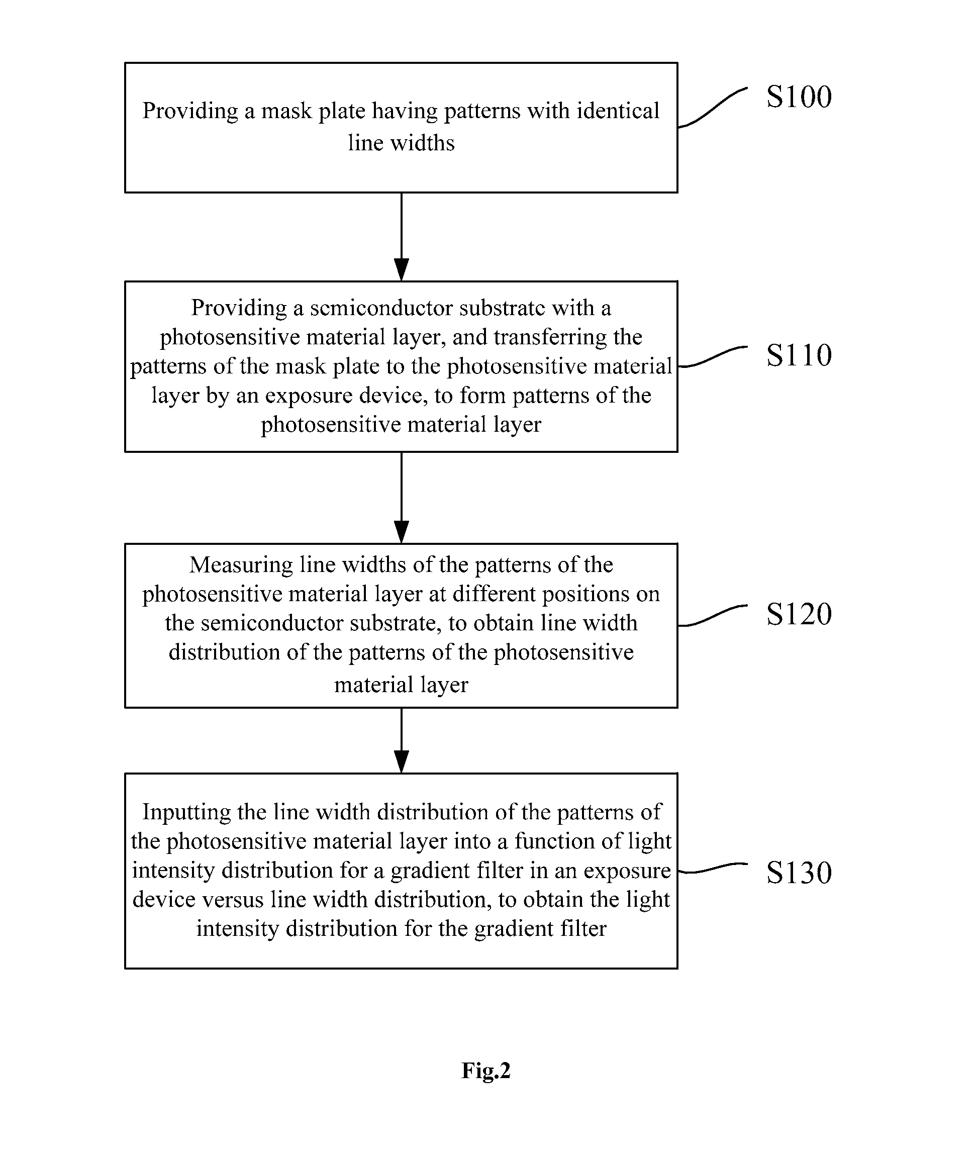
Method for Detecting Light Intensity Distribution for Gradient Filter and Method for Improving Line Width Consistency
a gradient filter and light intensity distribution technology, applied in the field of semiconductor manufacturing, can solve the problems of increasing manufacturing cost, complicated testing process, and having to shut down the exposure device, so as to improve the up time of the exposure device and reduce the cost. , the effect of saving tim
- Summary
- Abstract
- Description
- Claims
- Application Information
AI Technical Summary
Benefits of technology
Problems solved by technology
Method used
Image

Examples
Embodiment Construction
[0050]Hereinafter, the present invention will be further described in detail in conjunction with the embodiments thereof, with reference to the accompanying drawings.
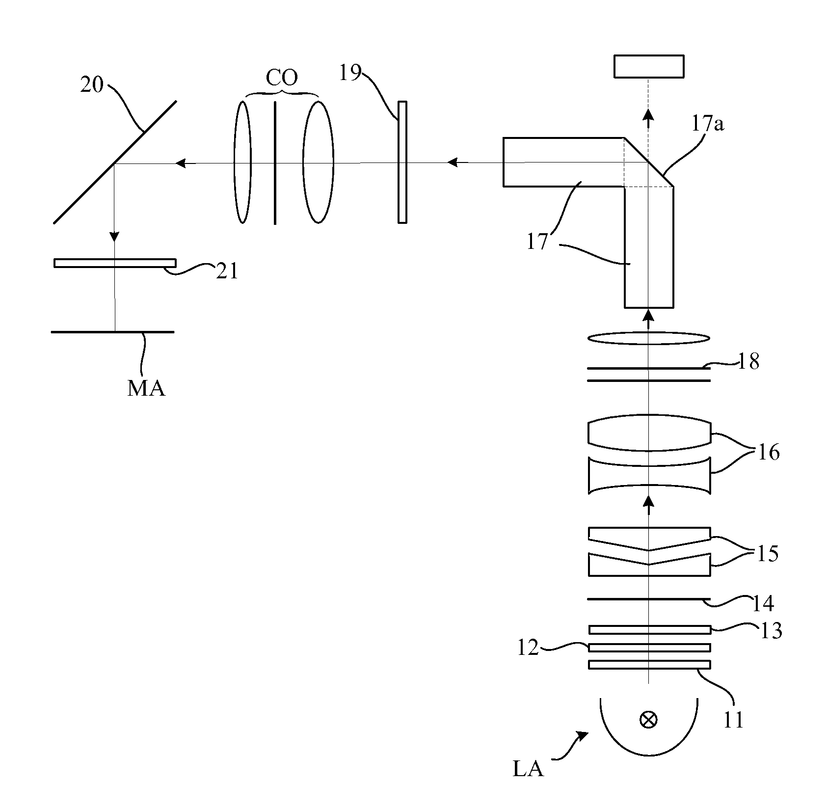
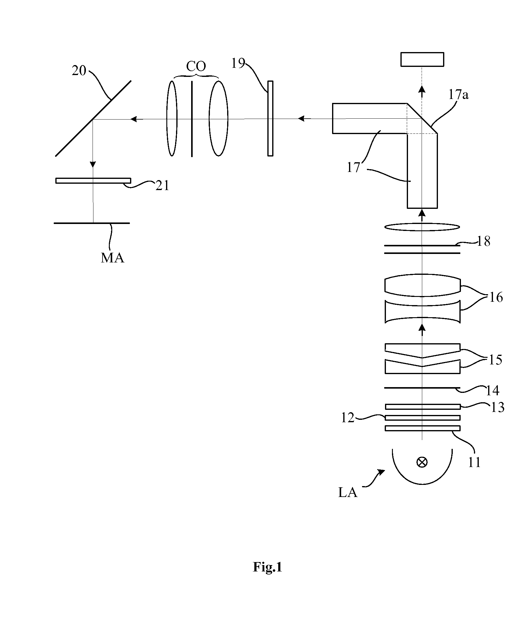
[0051]In a photolithography process, the patterns of the mask plate must be duplicated precisely to the photosensitive material layer on the semiconductor substrate. As for the same mask plate, it is necessary for the patterns of the photosensitive material layer to have identical line widths after the patterns of the mask plate are transferred to the photosensitive material layer on the semiconductor substrate, i.e., it is desirable that the light from the light source is distributed uniformly to each sections on the mask plate after passing through the optical system in the exposure device.
[0052]Due to the effect of aberration in the optical system, after the patterns of the mask plate with identical line widths are transferred to the photosensitive material layer by means of exposure, the patterns formed on the photo...
PUM
 Abstract
Description
Claims
Application Information