Array base plate, display panel and display device

A technology for array substrates and substrate substrates, applied in optics, instruments, character and pattern recognition, etc., can solve the problems affecting the accuracy of fingerprint recognition and the size of the photocurrent of the photosensitive structure, so as to avoid interference and improve the production yield , The effect of simplifying the preparation process

Active Publication Date: 2020-02-04
XIAMEN TIANMA MICRO ELECTRONICS
View PDF5 Cites 10 Cited by
  • Summary
  • Abstract
  • Description
  • Claims
  • Application Information

AI Technical Summary

Problems solved by technology

[0004] Usually, the array substrate includes a plurality of photosensitive structures, and each photosensitive structure is used to receive the light reflected back from the corresponding fingerprint identification area directly above it. If the crosstalk light reflected from the adjacent fingerprint identification area is reflected on the photosensitive structure, It will affect the size of the photocurrent generated by the photosensitive structure, and then affect the accuracy of fingerprint recognition

Method used


Image

  • Array base plate, display panel and display device
  • Array base plate, display panel and display device
  • Array base plate, display panel and display device

Examples


Embodiment Construction

[0040] The present invention will be further described in detail below in conjunction with the accompanying drawings and embodiments. It should be understood that the specific embodiments described here are only used to explain the present invention, but not to limit the present invention. In addition, it should be noted that, for the convenience of description, only some structures related to the present invention are shown in the drawings but not all structures.

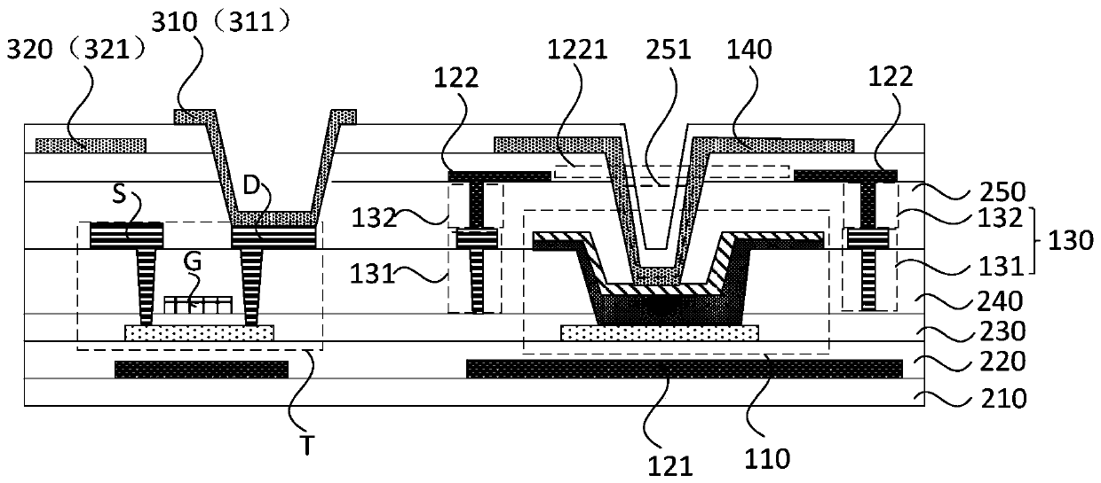
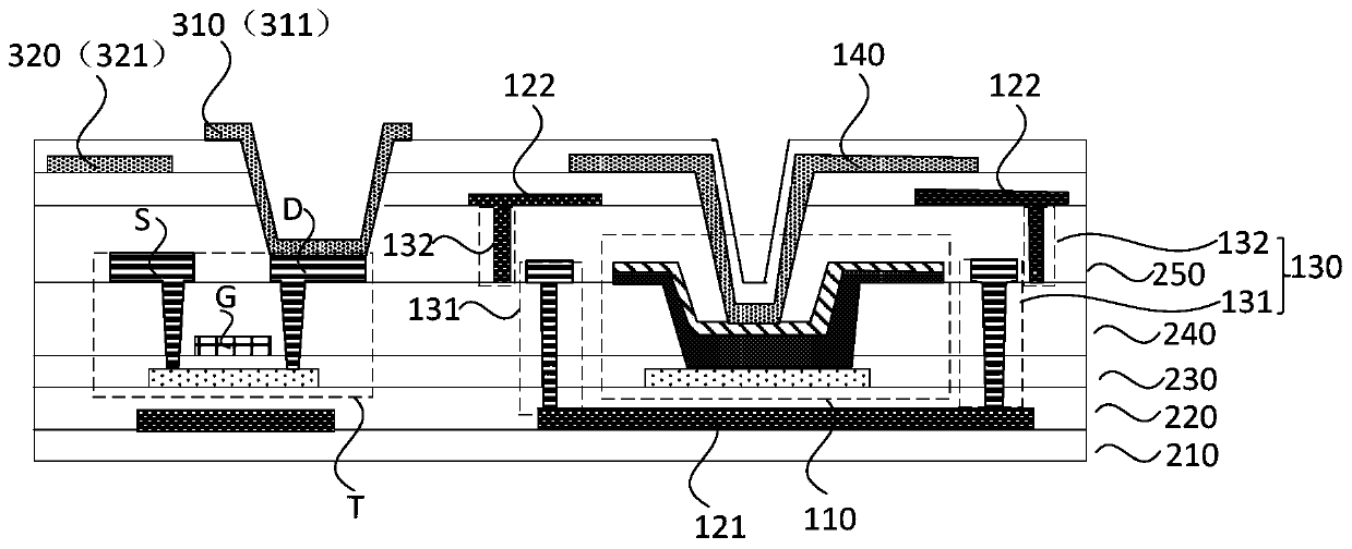
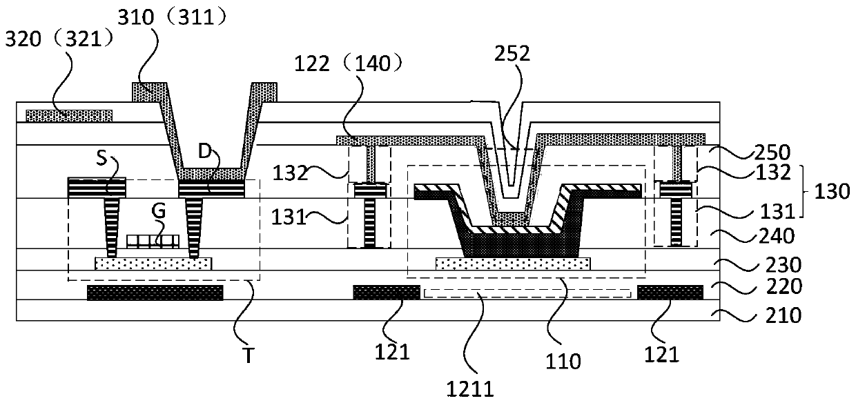
[0041] figure 1 is an array substrate provided by an embodiment of the present invention, see figure 1 , the array substrate includes: a base substrate 210 and a first light-shielding layer 121 located on one side of the base substrate 210; a photosensitive structure 110 located on a side of the first light-shielding layer 121 away from the base substrate 210; a second light-shielding layer 122 , located on the side of the light-sensitive structure 110 away from the base substrate 210; the light-shielding structu...


PUM


Abstract

The embodiment of the invention discloses an array base plate, a display panel and a display device. The array base plate includes: a substrate base plate; a first light-shielding layer, which is located at one side of the substrate base plate; a light-sensitive structure, which is located at one side that is of the first light-shielding layer and faces away from the substrate base plate; a secondlight-shielding layer, which is located at one side that is of the light-sensitive structure and faces away from the substrate base plate; and a light-shielding structure, which is located between the first light-shielding layer and the second light-shielding layer. In a direction perpendicular to the substrate base plate, the light-shielding structure surrounds the light-sensitive structure, andthe light-shielding structure includes at least a first light-shielding sub-part and a second light-shielding sub-part. The first light-shielding sub-part is located at one side close to the first light-shielding layer. The first light-shielding sub-part and the second light-shielding sub-part are prepared and formed by using different preparation processes. According to the technical solution provided by the invention, crosstalk light rays can be prevented from entering the light-sensitive structure, accuracy of fingerprint recognition is improved, at the same time, the light-shielding structure includes the first light-shielding sub-part and the second light-shielding sub-part, and preparation technology difficulty of the light-shielding structure can be reduced.

Description

technical field [0001] Embodiments of the present invention relate to the field of display technology, and in particular, to an array substrate, a display panel, and a display device. Background technique [0002] At present, in-screen fingerprint recognition, that is, embedding a fingerprint recognition device into the display area, is a research hotspot in the current display field. Embedding the fingerprint recognition device from the non-display area into the display area is conducive to improving the screen-to-body ratio of the display. [0003] Existing fingerprint identification technologies include optical fingerprint identification technology, semiconductor silicon fingerprint identification technology and ultrasonic fingerprint identification technology. Among them, the optical fingerprint recognition technology generally uses a photodiode as the light-sensing structure. Its working principle is: the reflected light formed after the light is reflected by the touch ...

Claims


Application Information

Patent Timeline
Patent Type & Authority Applications(China)
IPC IPC(8): G02F1/1362G06K9/00G06K9/20
CPCG02F1/136209G06V40/1318G06V10/147G02F1/133512G02F1/136218G02F1/136227G02F1/133357G02F1/133345G02F1/13338
Inventor 杨栩刘博智陈国照
Owner XIAMEN TIANMA MICRO ELECTRONICS
Why Eureka
Try Eureka