Method for preparing display substrate and display substrate

A technology for display substrates and display panels, which is used in semiconductor/solid-state device manufacturing, identification devices, semiconductor/solid-state device components, etc., can solve problems such as affecting the display effect of the display screen, and achieve the effect of avoiding the reduction of reflection efficiency

Active Publication Date: 2021-08-31
YUNGU GUAN TECH CO LTD
View PDF2 Cites 0 Cited by
  • Summary
  • Abstract
  • Description
  • Claims
  • Application Information

AI Technical Summary

Problems solved by technology

The protective film layer is generally a conductive material. If there is any conductive material on the pixel electrode, it may make the adjacent pixel electrodes electrically connected and affect the display effect of the display.

Method used


Image

  • Method for preparing display substrate and display substrate
  • Method for preparing display substrate and display substrate
  • Method for preparing display substrate and display substrate

Examples


Embodiment Construction

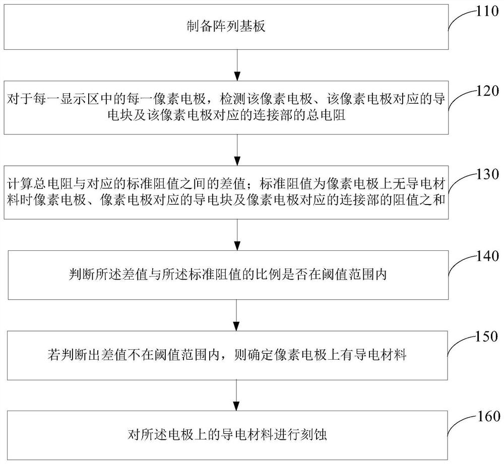
[0054] Reference will now be made in detail to the exemplary embodiments, examples of which are illustrated in the accompanying drawings. When the following description refers to the accompanying drawings, the same numerals in different drawings refer to the same or similar elements unless otherwise indicated. The implementations described in the following exemplary embodiments do not represent all implementations consistent with this application. Rather, they are merely examples of means consistent with aspects of the present application as recited in the appended claims.

[0055] As mentioned in the background art, a protective film layer is formed on the pixel electrodes of the pixels in the display screen before opening the holes. After opening, the protective film layer is removed. Generally, wet etching can be used to remove the protective film layer, but due to fluctuations in process conditions or a decrease in the concentration of the etchant in the later stages of ...


PUM


Abstract

The present application provides a method for preparing a display substrate and the display substrate. The preparation method includes: preparing an array substrate, the array substrate includes a plurality of display panel areas arranged at intervals and a peripheral area, and the peripheral area is provided with a test area corresponding to the plurality of display panel areas; There are a plurality of pixel electrodes, each test area is provided with a conductive block corresponding to the plurality of pixel electrodes in the corresponding display area, and the conductive block is electrically connected to the corresponding pixel electrode through the connecting part; for each display area For each pixel electrode, detect the total resistance value of the pixel electrode, the conductive block corresponding to the pixel electrode and the connection part corresponding to the pixel electrode; calculate the difference between the total resistance value and the corresponding standard resistance value; determine the difference between the difference value and the standard resistance value Whether the ratio of the resistance values ​​is within the threshold range; if it is judged that the ratio is not within the threshold range, it is determined that there is a conductive material on the pixel electrode; and etching the conductive material on the pixel electrode.

Description

technical field [0001] The present application relates to the field of display technology, in particular to a method for preparing a display substrate and the display substrate. Background technique [0002] With the rapid development of electronic devices, users have higher and higher requirements for screen-to-body ratio, so that the full-screen display of electronic devices has attracted more and more attention from the industry. Traditional electronic devices such as mobile phones and tablet computers need to integrate front-facing cameras, earpieces, and infrared sensing elements. Generally, holes are opened on the display screen, and cameras, earpieces, and infrared sensing elements are arranged in the opening area. [0003] In the process of preparing the display screen, before the hole is drilled, a protective film layer is generally formed on the pixel electrode of the pixel in the display screen, and the protective film layer is removed after the hole is opened to ...

Claims


Application Information

Patent Timeline
Patent Type & Authority Patents(China)
IPC IPC(8): H01L21/84H01L23/544H01L27/12G09F9/30
CPCG09F9/30H01L22/32H01L27/124H01L27/1259
Inventor 马红星李素华黄毅颜衡任佳佩胡庆元宫雪茹
Owner YUNGU GUAN TECH CO LTD
Why Eureka
Try Eureka