
Wafer film thickness detection method and edge washing boundary detection method

A detection method and layer thickness technology, which can be used in semiconductor/solid-state device testing/measurement, electrical components, circuits, etc., to solve the problems of delayed detection results, inability to obtain the thickness of wafer film layers, etc., to achieve easy access and easy edge cleaning Boundary, simple process effect

Inactive Publication Date: 2020-02-07
SHANGHAI HUALI MICROELECTRONICS CORP
View PDF14 Cites 1 Cited by
  • Summary
  • Abstract
  • Description
  • Claims
  • Application Information

AI Technical Summary

Problems solved by technology

[0005] The object of the present invention is to provide a method for detecting the thickness of the wafer film layer and a method for detecting the edge edge, so as to solve the problems in the prior art that the detection results are delayed and the thickness of the wafer film layer cannot be obtained.

Method used


Image

  • Wafer film thickness detection method and edge washing boundary detection method
  • Wafer film thickness detection method and edge washing boundary detection method
  • Wafer film thickness detection method and edge washing boundary detection method

Examples


Embodiment Construction

[0031] In order to make the object and features of the present invention more obvious and easy to understand, the technical solutions of the wafer film layer thickness detection method and the edge cleaning boundary detection method proposed by the present invention will be described in detail below in conjunction with the accompanying drawings. The present invention can be realized in different forms , should not be limited to the described embodiments. In addition, it should be noted that all the drawings are in a very simplified form and use inaccurate scales, which are only used to facilitate and clearly assist the purpose of illustrating the embodiments of the present invention.

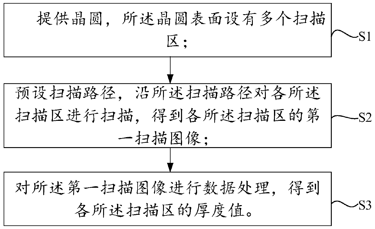
[0032] Please refer to figure 1 , figure 1 It is a schematic flow chart of the wafer film thickness detection method provided by the embodiment of the invention; the embodiment of the present invention provides a wafer film thickness detection method, comprising the following steps:

[0033] S...


PUM


Abstract

The invention provides a wafer film thickness detection method and an edge washing boundary detection method. The wafer film thickness detection method is characterized by arranging a plurality of scanning areas on the surface of a wafer; presetting a scanning path, and scanning each scanning area along the scanning path to obtain a first scanning image of each scanning area; and performing data processing on the first scanning image to obtain a thickness value of each scanning area. The method is simple in process, and can quickly obtain the thickness value of the wafer film layer. Moreover,the edge washing boundary detection method is characterized by carrying out difference calculation on the thickness values of the two adjacent scanning areas; comparing the difference value with a preset threshold value, and obtaining an edge washing boundary according to the comparison result; and if the difference value is not within the preset threshold value, judging that the scanning edge between the two scanning areas is the edge washing boundary. Therefore, the edge washing boundary can be conveniently obtained.

Description

technical field [0001] The invention relates to the technical field of semiconductor manufacturing, in particular to a method for detecting the thickness of a wafer film layer and a method for detecting an edge-washing boundary. Background technique [0002] In today's semiconductor manufacturing process, as the size of semiconductor manufacturing technology continues to shrink, in the wafer manufacturing process, the uniformity of wafer film growth is particularly important, especially affecting the exposure capability of the lithography process. The thickness is inspected to avoid the problems of yield reduction and cost increase caused by defects. [0003] For the detection of the edge washing boundary of the wafer, the current method is to collect the original image of the wafer edge, confirm the edge washing boundary characteristics, and then perform image processing on the original image by reducing pixels and stitching discrete pixels according to the known boundary i...

Claims


Application Information

Patent Timeline
IPC IPC(8): H01L21/66
CPCH01L22/12
Inventor 冯亚丽
Owner SHANGHAI HUALI MICROELECTRONICS CORP
Learn More