A large-size light-emitting diode with invisible extended electrodes and its manufacturing method

A technology of light-emitting diodes and extended electrodes, which is applied in circuits, electrical components, semiconductor devices, etc., can solve the problems of not being suitable for large-sized light-emitting diodes, jagged edges of extended electrodes or shedding of extended electrodes, and reduced luminous efficiency, so as to achieve superior current The effect of the extended effect

Active Publication Date: 2020-11-24
XIAMEN CHANGELIGHT CO LTD
View PDF8 Cites 0 Cited by
  • Summary
  • Abstract
  • Description
  • Claims
  • Application Information

AI Technical Summary

Problems solved by technology

[0003] However, the large-scale chip adopts a chip electrode structure with multiple extended currents. Although the current can be spread better in large-area chips, more extended electrodes are needed for guidance, and the light-emitting diodes of GaN-based materials on the sapphire substrate are on the same side. electrode, so that the light-blocking area of ​​the extended electrode on both sides of P and N and the loss area of ​​the active area increase to reduce the luminous efficiency
[0004] In the prior art, such as the patent No. 201410433643.5 discloses an infrared light-emitting diode with embedded extended electrodes, which forms a groove on the roughened layer and exposes the ohmic contact layer, and the extended electrode is formed on the ohmic contact layer in the groove On the surface, the extended electrode is in contact with the ohmic contact layer to form an ohmic contact. The main technical effect is that the extended electrode is formed by filling the trench with metal, which solves the problem of lateral etching of the epitaxial layer under the extended electrode caused by the removal of the epitaxial layer or surface roughening layer, resulting in The technical problem of jagged edges of the extended electrodes or the extended electrodes falling off. In addition, the patent also describes that the shape of the groove is in the shape of "one" or "ten". The groove is filled with extended electrodes, so whether it is a "one" or "ten" shaped groove, the extended electrodes will directly block the light-emitting area at the bottom of the groove, which affects the luminous efficiency, and is not suitable for large-sized light-emitting diodes.

Method used


Image

  • A large-size light-emitting diode with invisible extended electrodes and its manufacturing method
  • A large-size light-emitting diode with invisible extended electrodes and its manufacturing method
  • A large-size light-emitting diode with invisible extended electrodes and its manufacturing method

Examples


Embodiment Construction

[0047] In order to more clearly illustrate the technical solutions in the embodiments of the present invention or the prior art, the following will briefly introduce the drawings that need to be used in the description of the embodiments or the prior art. Obviously, the accompanying drawings in the following description are only These are some embodiments of the present invention. For those of ordinary skill in the art, other drawings can also be obtained according to these drawings without paying creative labor. Please refer to Figure 1 to Figure 15 .

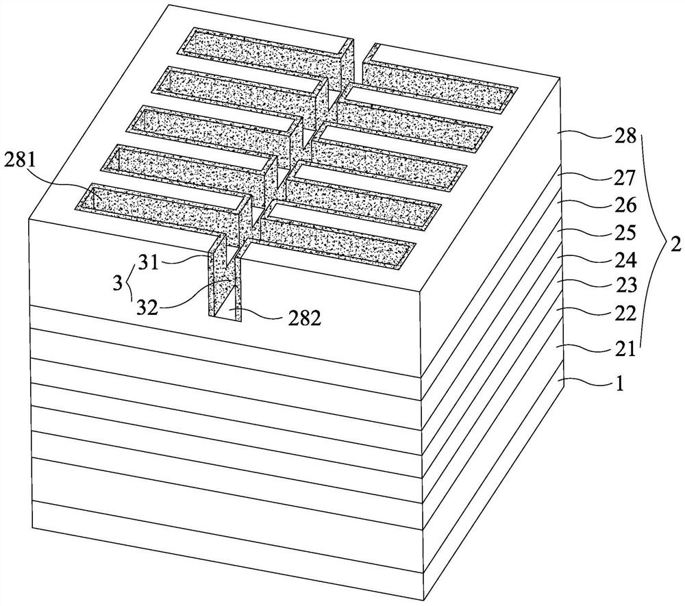
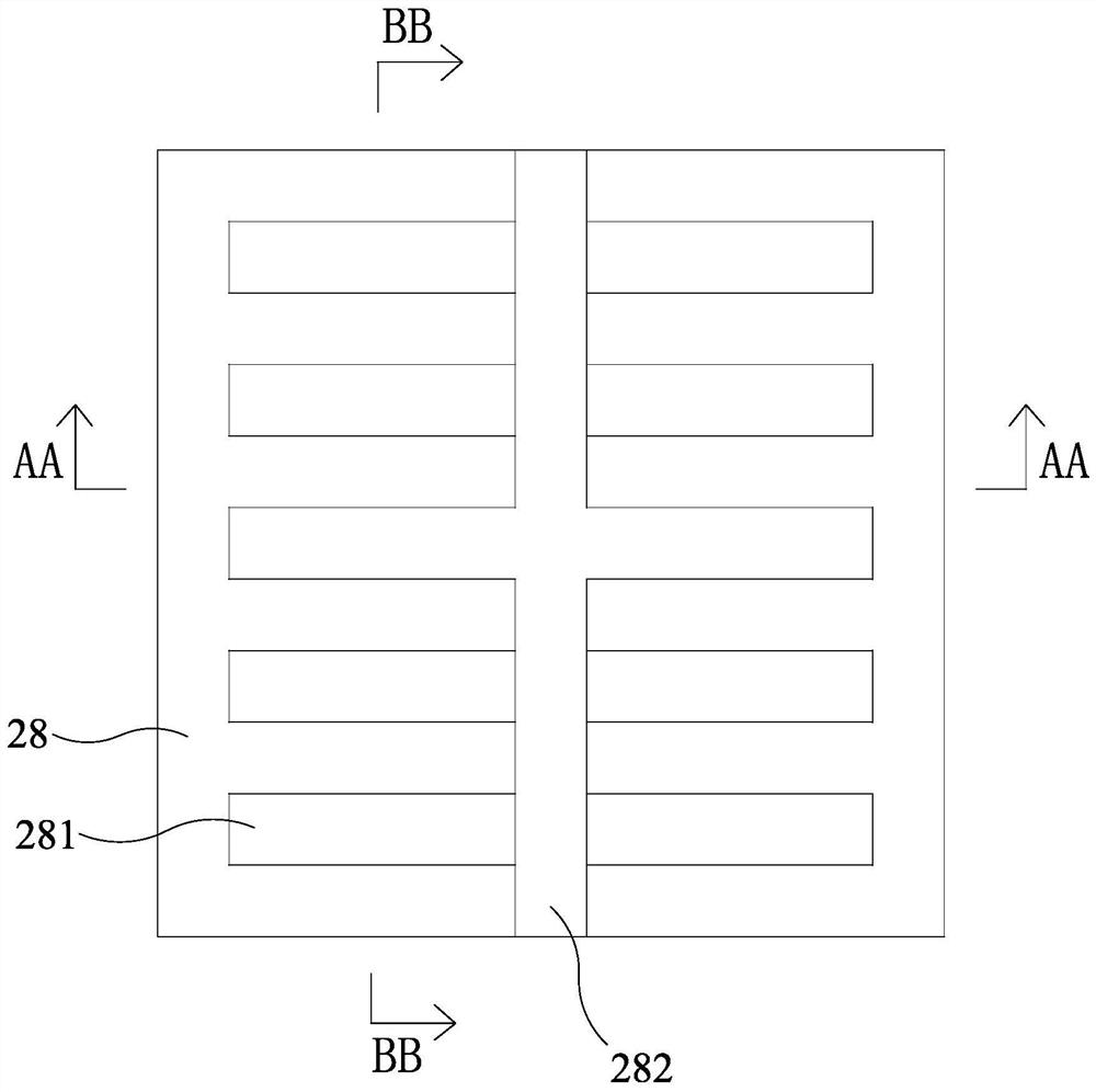
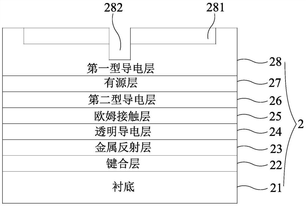
[0048] The following is an example of a light-emitting diode with a vertical structure, such as Figure 7 As shown, the present invention discloses a large-sized light-emitting diode with invisible extended electrodes, including a first electrode composed of a second electrode 1 , an epitaxial structure 2 , and a soldering station electrode 4 connected to a metal extended electrode 3 .

[0049] Such as image 3 and Figure...


PUM


Abstract

The invention discloses a large-sized LED with a concealed extension electrode. The large-sized LED includes an epitaxial structure, a second electrode, and a first electrode composed of a solder padelectrode connected to a metal extension electrode. The epitaxial structure includes a substrate, a second type of conductive layer, an active layer and a first type of conductive layer. The second type of conductive layer is electrically connected to the second electrode. A groove is formed in the first type of conductive layer. The side walls of the groove form metal extension electrode layers.The metal extension electrode layers of the adjacent side walls are continuous with each other. The solder pad electrode is arranged in the groove. The solder pad electrode and the metal extension electrode layers are electrically connected to each other. The invention also discloses a manufacturing method of the LED. A special groove structure is provided to achieve an effect of uniformly expanding the current. The extension electrode has an extremely low thickness, and is arranged on the vertical surface on the side of the groove, which is equivalent to being invisible. The large-sized LED solves the problem that the bottom surface of a metal extension electrode in the prior art shields light, and realizes a wide range of light emitting area, thereby maintaining a superior current spreading effect.

Description

technical field [0001] The invention relates to the field of light-emitting diodes, in particular to a large-size light-emitting diode with invisible extended electrodes and a manufacturing method. Background technique [0002] With the rapid development of light-emitting diodes, the application of LEDs is changing with each passing day. As the market demands more and more light-emitting power for light-emitting diodes, the chip size is also getting bigger and bigger. Due to the problem of insufficient current expansion caused by large-size chips, the chip structure is continuously improved and optimized. At present, large-size chips all adopt a chip electrode structure with multiple expansion currents, so that the current can be better expanded in large-area chips. [0003] However, the large-scale chip adopts a chip electrode structure with multiple extended currents. Although the current can be spread better in large-area chips, more extended electrodes are needed for g...

Claims


Application Information

Patent Timeline
Patent Type & Authority Patents(China)
IPC IPC(8): H01L33/38H01L33/00
CPCH01L33/005H01L33/38H01L2933/0016
Inventor 林志伟陈凯轩蔡建九曲晓东赵斌
Owner XIAMEN CHANGELIGHT CO LTD
Why Eureka
Try Eureka