Wafer Inversion Integrated LED Display Packaging Module

A wafer-inverted, packaged module technology, applied in electrical components, electro-solid devices, circuits, etc., can solve the problems of reduced light output rate of LED wafers, occupying module production time, low structural mechanical strength, etc., to improve light output rate. , Speed ​​up heat dissipation, save the effect of wire bonding process

Active Publication Date: 2017-01-18
CHANGCHUN CEDAR ELECTRONICS TECH CO LTD
View PDF4 Cites 0 Cited by
  • Summary
  • Abstract
  • Description
  • Claims
  • Application Information

AI Technical Summary

Problems solved by technology

[0003] In the above structure, the connecting wire has the disadvantages of long lead path and too small cross-sectional area, resulting in excessive heat generation and low mechanical strength of the structure
Moreover, because the electrodes on the wafer block part of the light-emitting area, the light output rate of the LED wafer is reduced, which affects the display brightness.
In addition, the current wire bonding process takes up a lot of module production time, resulting in a decrease in production efficiency and an increase in cost.

Method used


Image

  • Wafer Inversion Integrated LED Display Packaging Module
  • Wafer Inversion Integrated LED Display Packaging Module
  • Wafer Inversion Integrated LED Display Packaging Module

Examples


Embodiment 1

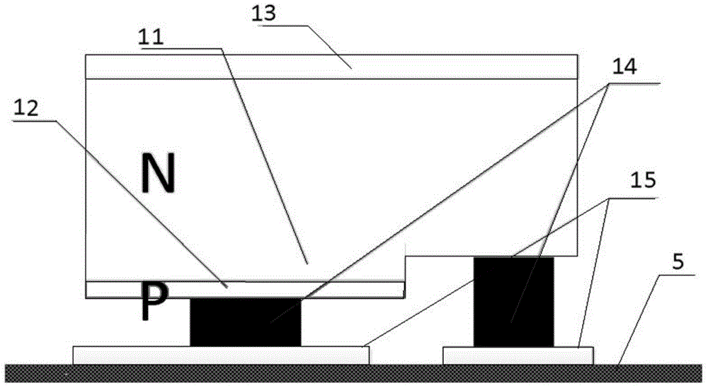
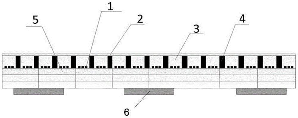
[0031] Such as figure 2 As shown, the inverted wafer integrated LED display packaging module of the present invention includes: a driver IC 6 , a driver circuit board 5 , an LED wafer 1 , a mask 4 , a transparent potting colloid 3 , and a translucent modified film 2 . The dot pitch is d=1mm, and the resolution is 64×64. The drive IC 6 is welded on the back of the drive circuit board 5, and the LED wafer 1 is fixed on the front of the drive circuit board 5; the blue and green LED chips are installed upside down, and the red LED chips are installed upright; the dimensions of the blue and green LED chips are: 8mils×8mils, the positive and negative electrodes of the blue and green LED chips are connected and fixed to the corresponding printed electrodes on the drive circuit board 5 through conductive silver glue, and the conductive silver glue required to fix each electrode is about: 0.0015mm -3 The position of the mask 4 corresponding to the LED wafer 1 has a light outlet, and ...

Embodiment 2

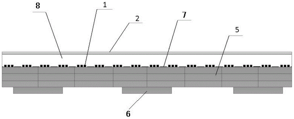
[0033] Such as image 3 As shown, the inverted wafer integrated LED display packaging module of the present invention includes: a driver IC 6 , a driver circuit board 5 , an LED wafer 1 , a black paint layer 7 , a transparent protective adhesive layer 8 , and a light-transmitting modified film 2 . The dot pitch is d=1.5mm, and the resolution is 64×64. The driver IC 6 is welded on the back of the driver circuit board 5, and the LED wafer 1 is fixed on the front of the driver circuit board 5; the blue and green LED chips are installed upside down, and the red LED chips are installed upright; the size of the blue and green LED chips is: 7mils ×12mils, the positive and negative electrodes of the blue and green LED chips are connected and fixed to the corresponding electrodes on the drive circuit board 5 through conductive silver glue, and the conductive silver glue required to fix each electrode is about: 0.003mm -3 The front of the driving circuit board 5 is sprayed with a black...

Embodiment 3

[0035] Such as image 3 As shown, the inverted wafer integrated LED display packaging module of the present invention includes: a driver IC 6 , a driver circuit board 5 , an LED wafer 1 , a black paint layer 7 , a transparent protective adhesive layer 8 , and a light-transmitting modified film 2 . The dot pitch is d=1.5mm, and the resolution is 64×64. The driver IC 6 is welded on the back of the driver circuit board 5, and the LED wafer 1 is fixed on the front of the driver circuit board 5; the blue and green LED chips are installed upside down, and the red LED chips are installed upright; the size of the blue and green LED chips is: 7mils ×12mils, the positive and negative electrodes of the blue and green LED chips are connected and fixed to the corresponding electrodes on the drive circuit board through conductive silver glue, and the conductive silver glue required to fix each electrode is about: 0.002mm -3The front of the driving circuit board 5 is sprayed with a black pa...


PUM


Abstract

The invention relates to an integrated LED displaying packaging module with LED chips arranged in wafers in an inverted mode. The integrated LED displaying packaging module comprises a drive circuit board and the LED wafers. The LED wafers are fixed to the drive circuit board. The LED chips of at least one primary color in the LED wafers are arranged in the inverted mode, positive electrodes of the LED chips and a positive electrode printed on the drive circuit board are fixed together in a bonding mode through conductive silver adhesives, and negative electrodes of the LED chips and a negative electrode printed on the drive circuit board are fixed together in a bonding mode through conductive silver adhesives. Transparent substrates are adopted for the LED chips arranged in the inverted mode. Most trivial welding processes are omitted, production time and cost are reduced, the phenomenon that light is shielded by electrodes under forward situations is avoided, and light emitting efficiency is improved. Because the electrodes of the chips are connected with the drive circuit board through the conductive silver adhesives, the defect that a connecting wire is long in guide passage and too small in cross section area is overcome, heat dissipation is accelerated, and structural mechanical strength is also improved.

Description

technical field [0001] The invention belongs to the technical field of LED flat panel display, and relates to an integrated LED display packaging module with wafer upside-down installation. Background technique [0002] The integrated LED display module includes an LED display module composed of a driver IC, a driver circuit board, and red, green, and blue primary color LED wafers. The current common practice is: solder the driver IC on the back of the driver circuit board, place the LED chip upright and fix it on the corresponding pixel position on the front surface of the driver circuit board through an adhesive, and then connect the blue and green LED chips by wire bonding. The positive and negative electrodes and the positive electrode of the red LED crystal unit (single electrode) are connected to the corresponding circuit position of the circuit board by welding the connecting wire (gold wire or aluminum wire), and finally sealant and mask protection are carried out on...

Claims


Application Information

Patent Timeline
Patent Type & Authority Patents(China)
IPC IPC(8): H01L25/16H01L33/48H01L33/62
CPCH01L2224/16225
Inventor 王瑞光田志辉邓意成郑喜凤陈宇严飞
Owner CHANGCHUN CEDAR ELECTRONICS TECH CO LTD
Why Eureka
Try Eureka