Display panel

A technology for display panels and substrates, applied in semiconductor devices, electrical components, photovoltaic power generation, etc., can solve the problems of metal wiring breakage in the bending area, reducing the reliability of the display panel, uncontrollable bending radius, etc. ratio, the effect of reducing the border width, and reducing the bend radius

Active Publication Date: 2020-02-14
WUHAN CHINA STAR OPTOELECTRONICS SEMICON DISPLAY TECH CO LTD
View PDF19 Cites 3 Cited by
  • Summary
  • Abstract
  • Description
  • Claims
  • Application Information

AI Technical Summary

Problems solved by technology

[0005] An object of the present invention is to provide a display panel, which can solve the problem that the bending radius of the existing display panel is uncontrollable when bending the bending area, which easily leads to the breakage of the metal wiring in the bending area, reducing the The reliability of the display panel, etc.

Method used


Image

  • Display panel
  • Display panel
  • Display panel

Examples


Embodiment 1

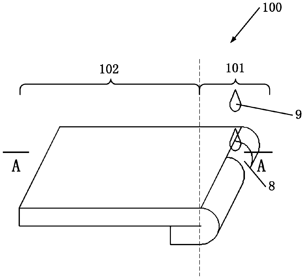
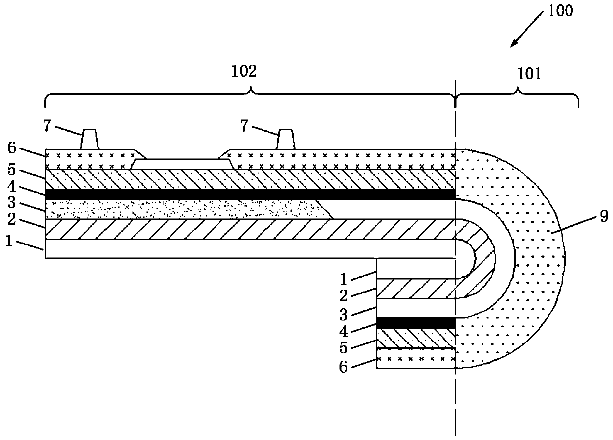
[0042] like figure 1 , figure 2 As shown, a display panel 100 is defined with a bending area 101 and a non-bending area 102, which includes: a substrate 1, a semiconductor device layer 2, an insulating layer 3, a source and drain layer 4, a flat layer 5, and a pixel definition layer 6 and support column 7.

[0043] Wherein the semiconductor device layer 2 is disposed on the substrate 1 . Specifically, the semiconductor device layer 2 includes: an active layer, a gate insulating layer, and a gate layer. Wherein the active layer is disposed on the substrate; the gate insulating layer is disposed on the active layer; the gate layer is disposed on the gate insulating layer; details will not be repeated here.

[0044] The insulating layer 3 is disposed on the semiconductor device layer 2; specifically, the insulating layer 3 is disposed on the gate layer. The insulating layer 3 mainly plays an insulating role, preventing the source-drain layer 4 from directly contacting the ga...

Embodiment 2

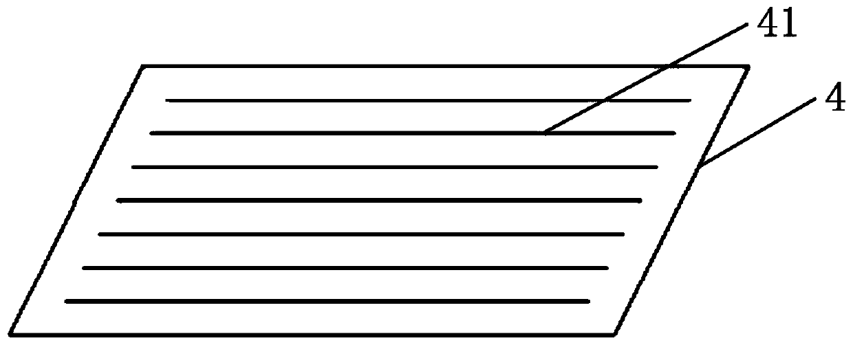
[0052] like Figure 4 , Figure 5 As shown, the display panel 100 in this embodiment further includes a backing plate 10 , and the backing plate 10 is disposed on a side of the substrate 1 away from the source-drain layer 4 . In this embodiment, the shape of the contact side surface between the backing plate 10 and the substrate 1 after bending is rectangular. Wherein the groove 8 can go through the pixel definition layer 6, the planar layer 5 to the source and drain layer 4, and then fill the groove 8 with conductive material, thereby connecting the metal wiring 41, so that The metal wiring 41 in the bending area 101 does not need to consider the stress balance problem, thereby reducing the bending radius, reducing the frame width, increasing the screen-to-body ratio, and finally bringing better visual experience to customers.

[0053] like Image 6 , Figure 7 As shown, more preferably, the backing plate 10 is provided with conductive bridges 11 at intervals correspondin...

Embodiment 3

[0056] like Figure 8 , Figure 9 As shown, the difference between this embodiment and Embodiment 2 lies in that: the display panel 100 further includes a backing plate 10 , and the backing plate 10 is disposed on a side of the substrate 1 away from the source-drain layer 4 . In this embodiment, the shape of the contact side surface of the backing plate 10 and the substrate 1 after bending is arc-shaped. Wherein the groove 8 can go through the pixel definition layer 6, the planar layer 5 to the source and drain layer 4, and then fill the groove 8 with conductive material, thereby connecting the metal wiring 41, so that The metal wiring 41 in the bending area 101 does not need to consider the stress balance problem, thereby reducing the bending radius, reducing the frame width, increasing the screen-to-body ratio, and finally bringing better visual experience to customers.

[0057] like Figure 10 As shown, more preferably, wherein the backing plate 10 is provided with condu...


PUM


Abstract

The invention relates to a display panel. On the one hand, a groove is formed in the position, which corresponds to metal wires, of a source and drain electrode layer of a bending area, the groove isfilled with a conductive material, the metal wires are connected through the conductive material, so that the metal wires in the bending area do not need to consider the problem of stress balance, thebending radius is reduced, the frame width is reduced, the screen-to-body ratio is improved, and finally better visual experience is brought to customers. On the other hand, the display panel is further provided with a base plate, and the base plate is provided with conductive bridges arranged at the position corresponding to the groove at intervals, so that the metal wires can be better connected through the conductive bridges, and the phenomenon that the metal wires cannot be connected by the conductive material due to the fact that the metal wires are too thin is prevented.

Description

technical field [0001] The present invention relates to the field of display technology, in particular to a display panel. Background technique [0002] Organic light-emitting display device (English full name: Organic Light-Emitting Diode, referred to as OLED) is also called organic electro-laser display device, organic light-emitting semiconductor. The working principle of OLED is: when the power is supplied to an appropriate voltage, positive holes and cathode charges will combine in the light-emitting layer, and under the action of Coulomb force, they will recombine with a certain probability to form excitons in an excited state (electron-hole Right), and this excited state is unstable in the usual environment, the excitons in the excited state recombine and transfer energy to the luminescent material, making it transition from the ground state energy level to the excited state, and the excited state energy passes through the radiation relaxation process Generate photon...

Claims


Application Information

Patent Timeline
Patent Type & Authority Applications(China)
IPC IPC(8): H01L27/12H01L27/32
CPCH01L27/1244H10K59/12H10K59/131H01L27/1218H10K71/611H10K77/111H10K2102/311H10K59/122
Inventor 周阳蔡在秉
Owner WUHAN CHINA STAR OPTOELECTRONICS SEMICON DISPLAY TECH CO LTD
Why Eureka
Try Eureka