GeSn phototransistor based on III-V group material emitter region and manufacturing method thereof

A III-V, phototransistor technology, used in final product manufacturing, sustainable manufacturing/processing, circuits, etc., can solve problems such as low detection sensitivity, and achieve high sensitivity, large photocurrent magnification, and high optical gain.

Active Publication Date: 2020-02-21
SHANGHAI IND U TECH RES INST
View PDF3 Cites 1 Cited by
  • Summary
  • Abstract
  • Description
  • Claims
  • Application Information

AI Technical Summary

Problems solved by technology

[0005] The invention provides a GeSn phototransistor based on III-V group material emitter region and its manufacturing method, which is used to solve the problem of low detection sensitivity of GeSn phototransistor in the prior art, so as to improve the performance of GeSn phototransistor

Method used


Image

  • GeSn phototransistor based on III-V group material emitter region and manufacturing method thereof
  • GeSn phototransistor based on III-V group material emitter region and manufacturing method thereof
  • GeSn phototransistor based on III-V group material emitter region and manufacturing method thereof

Examples


no. 1 Embodiment approach

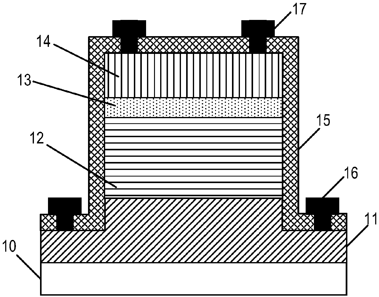
[0040] This specific embodiment provides a GeSn phototransistor based on the III-V group material emitter region, with figure 1 It is a structural schematic diagram of a GeSn phototransistor based on a III-V group material emitter region in the first embodiment of the present invention.

[0041] Such as figure 1 As shown, the GeSn phototransistor based on the emitter region of the III-V group material provided in this specific embodiment includes a substrate 10 and collectors stacked on the surface of the substrate 10 in sequence along a direction perpendicular to the substrate 10 Region 11, absorption layer 12, base region 13 and emitter region 14; the absorption layer 12 and the base region 13 use Ge 1-x sn x Composed of materials, wherein, 01-x sn x The lattice mismatch degree of the material is less than a preset value, and the energy bandgap of the III-V group material is larger than the Ge 1-x sn x Material.

[0042] In this specific embodiment, using Ge 1-x sn x...

no. 2 Embodiment approach

[0064] This specific embodiment provides a GeSn phototransistor based on the III-V group material emitter region, with Figure 4 It is a schematic structural diagram of a GeSn phototransistor based on a III-V group material emitter region in the second specific embodiment of the present invention. For the same parts as the first specific embodiment, this specific embodiment will not repeat it, and the differences from the first specific embodiment will be mainly described below.

[0065] Such as Figure 4 As shown, the GeSn phototransistor based on the emitter region of the III-V group material provided in this specific embodiment includes a substrate 40 and collectors sequentially stacked on the surface of the substrate 40 along a direction perpendicular to the substrate 40 Region 41, absorption layer 42, base region 43 and emitter region 44; the absorption layer 42 and the base region 43 use Ge 1-x sn x Composed of materials, wherein, 01-x sn x The lattice mismatch degre...


PUM

PropertyMeasurementUnit
thicknessaaaaaaaaaa
thicknessaaaaaaaaaa
thicknessaaaaaaaaaa

Abstract

The invention relates to the technical field of semiconductor manufacturing and particularly relates to a GeSn phototransistor based on an III-V group material emitter region and a manufacturing method thereof. The GeSn phototransistor based on the III-V group material emitter region comprises a substrate, and a collector region, an absorption layer, a base region and an emitter region which are sequentially stacked on a surface of the substrate in the direction perpendicular to the substrate, wherein the absorption layer and the base region are made of a Ge1-xSnx material, x is greater than 0and less than 1, the emitter region is made of a III-V group material, the lattice mismatch degree of the III-V group material and the Ge1-xSnx material is smaller than a preset value, and an energyband gap of the III-V group material is larger than that of the Ge1-xSnx material. The GeSn phototransistor is advantaged in that a phototransistor has a large photocurrent amplification multiple andhigh sensitivity, and high optical gain can be realized more easily.

Description

technical field [0001] The invention relates to the technical field of semiconductor manufacturing, in particular to a GeSn phototransistor based on a III-V group material emitter region and a manufacturing method thereof. Background technique [0002] GeSn, as a new group IV alloy material, has a large absorption coefficient in the near infrared and even short-wave infrared, and is an ideal material for preparing Si infrared photodetectors. In recent years, GeSn infrared photodetectors have been extensively studied. In their published paper entitled "Silicon-based Ge 0.89 sn 0.11 "photodetector and lightemitter towards mid-infrared applications" discloses a surface-receiving GeSn photodetector, a GeSn alloy with a Sn component content of 11% is used as an absorbing layer, and its photoresponse range extends to the 3um waveband. [0003] However, the sensitivity of conventional GeSn p-i-n photodetectors is limited due to the lack of internal gain mechanism. Authors such ...

Claims


Application Information

Patent Timeline
Patent Type & Authority Applications(China)
IPC IPC(8): H01L31/109H01L31/0336H01L31/18
CPCH01L31/0336H01L31/109H01L31/18Y02P70/50
Inventor 汪巍方青涂芝娟曾友宏蔡艳王庆王书晓余明斌
Owner SHANGHAI IND U TECH RES INST
Why Eureka
Try Eureka