Relaxation GeSn infrared avalanche photodetector and manufacturing method thereof

A technology of avalanche optoelectronics and manufacturing methods, which is applied in the direction of final product manufacturing, sustainable manufacturing/processing, circuits, etc., can solve the problem of low sensitivity of GeSn infrared photodetectors, and achieve the effect of high sensitivity and large photocurrent magnification

Active Publication Date: 2020-02-14
SHANGHAI IND U TECH RES INST
View PDF7 Cites 0 Cited by
  • Summary
  • Abstract
  • Description
  • Claims
  • Application Information

AI Technical Summary

Problems solved by technology

[0005] The invention provides a relaxation GeSn infrared avalanche photodetector and its manufacturing method, which is used to solve the problem of low sensitivity of the existing GeSn infrared photodetector

Method used


Image

  • Relaxation GeSn infrared avalanche photodetector and manufacturing method thereof
  • Relaxation GeSn infrared avalanche photodetector and manufacturing method thereof
  • Relaxation GeSn infrared avalanche photodetector and manufacturing method thereof

Examples


Embodiment Construction

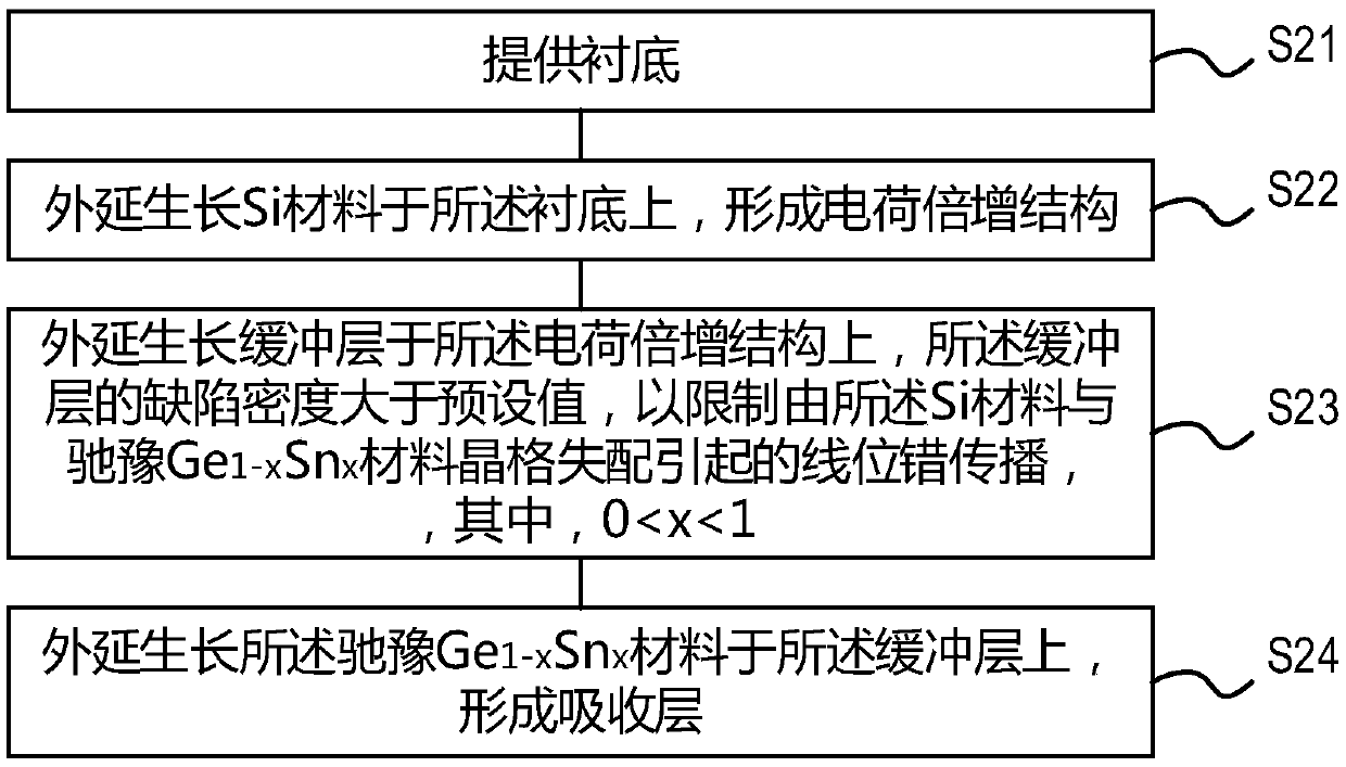
[0039] The specific implementation of the relaxation GeSn infrared avalanche photodetector and its manufacturing method provided by the present invention will be described in detail below in conjunction with the accompanying drawings.

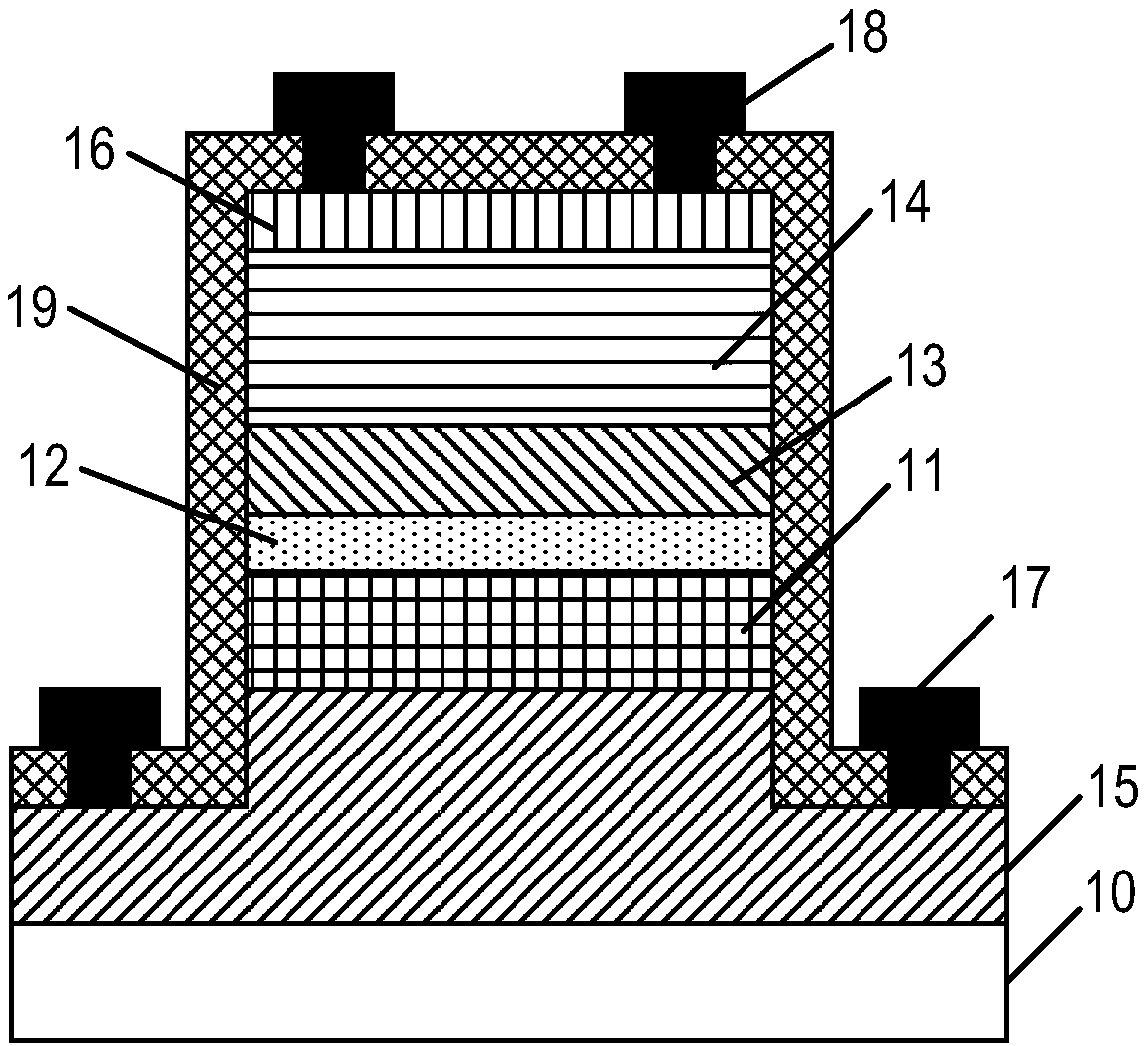
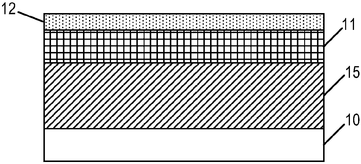
[0040] This specific embodiment provides a kind of relaxation GeSn infrared avalanche photodetector, with figure 1 It is a structural schematic diagram of a relaxed GeSn infrared avalanche photodetector in a specific embodiment of the present invention. Such as figure 1 As shown, the relaxed GeSn infrared avalanche photodetector provided in this specific embodiment includes a substrate 10 and a charge multiplication structure, a buffer layer 13 and an absorbing layer stacked on the substrate 10 in sequence along a direction perpendicular to the substrate 10. Layer 14; the charge multiplication structure is made of Si material; the absorption layer 14 is made of relaxed Ge 1-x sn x material, wherein, 01-x sn x Wire dislocation propagation du...


PUM

PropertyMeasurementUnit
thicknessaaaaaaaaaa
thicknessaaaaaaaaaa
thicknessaaaaaaaaaa

Abstract

The invention relates to the technical field of semiconductor manufacturing, and particularly relates to a relaxation GeSn infrared avalanche photodetector and a manufacturing method thereof. The relaxation GeSn infrared avalanche photodetector comprises a substrate, a charge multiplication structure, a buffer layer and an absorption layer, wherein the charge multiplication structure, the buffer layer and the absorption layer are sequentially stacked on the substrate in the direction perpendicular to the substrate; the charge multiplication structure is made of a Si material; the absorption layer is made of a relaxation Ge<1-x>Snx material, and x is greater than 0 and less than 1; and the buffer layer is made of a Si<1-y>Gey material, y is larger than 0.2 and less than 0.8, and the defectdensity of the buffer layer is greater than a preset value so as to limit line dislocation propagation caused by lattice mismatch of the Si material and the relaxation Ge<1-x>Snx material. The relaxation GeSn infrared avalanche photodetector has large photocurrent amplification multiple and high sensitivity, the growth of a thick relaxation Ge buffer layer is avoided, and defect dislocation is limited in the buffer layer, so that the growth of a high-quality relaxation GeSn absorption layer is guaranteed.

Description

technical field [0001] The invention relates to the technical field of semiconductor manufacturing, in particular to a relaxation GeSn infrared avalanche photodetector and a manufacturing method thereof. Background technique [0002] Infrared photodetectors are widely used in communication, night vision, guidance, astronomical observation, and biomedicine. Compared with traditional III-V and II-V infrared photodetectors, IV infrared photodetectors are small in size, easy to integrate, low in cost and high in performance because of their manufacturing process compatibility with Si-based CMOS technology. and other potential advantages. Ge detectors based on Si substrates or SOI (Silicon On Insulator, silicon-on-insulator) substrates have been widely used in the fields of communication and sensing. However, when the wavelength of Ge material is greater than 1.55 μm, the absorption coefficient drops sharply, which makes Ge detectors unable to meet the applications of short-wav...

Claims


Application Information

Patent Timeline
Patent Type & Authority Applications(China)
IPC IPC(8): H01L31/107H01L31/18H01L31/028
CPCH01L31/028H01L31/107H01L31/1804Y02P70/50
Inventor 汪巍方青涂芝娟曾友宏蔡艳王庆王书晓余明斌
Owner SHANGHAI IND U TECH RES INST
Why Eureka
Try Eureka