Supercharge Your Innovation With Domain-Expert AI Agents!

Method for manufacturing semiconductor device

A manufacturing method and semiconductor technology, applied in semiconductor devices, semiconductor/solid-state device manufacturing, electric solid-state devices, etc., can solve the problems of epitaxial layer loss, increased process cost and complexity, and unproven problems

Inactive Publication Date: 2020-02-25
TAIWAN SEMICON MFG CO LTD
View PDF0 Cites 3 Cited by
  • Summary
  • Abstract
  • Description
  • Claims
  • Application Information

AI Technical Summary

Problems solved by technology

So each additional mask used for a given process adds cost and complexity to the process
Additionally, in at least some existing examples, separate photolithography processes and separate masks are used to define epitaxial n-type source / drain regions and epitaxial p-type source / drain regions, which may also require deposition of and removal of additional masking layers (such as dielectric isolation layers), which cause epitaxial layer loss (such as epitaxial layer loss in n-type source / drain regions and p-type source / drain regions)
Therefore, the existing technology has not yet proved to fully meet the needs of all aspects

Method used


Image

  • Method for manufacturing semiconductor device
  • Method for manufacturing semiconductor device
  • Method for manufacturing semiconductor device

Examples


Embodiment Construction

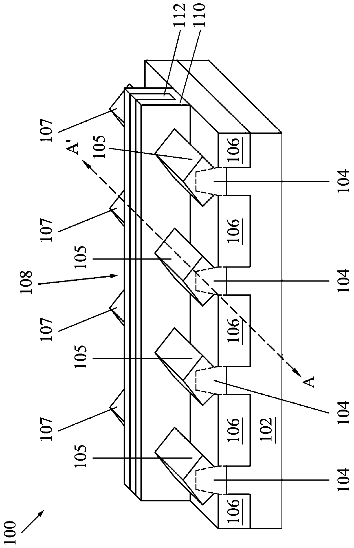
[0032] Different embodiments or examples provided below may implement different configurations of the present invention. The following examples of specific components and configurations are used to simplify the content of the present invention but not to limit the present invention. For example, a description of forming a first component on a second component includes an embodiment in which the two are in direct contact, or an embodiment in which the two are interposed by other additional components rather than in direct contact. On the other hand, multiple examples of the present invention may repeatedly use the same reference numerals for brevity, but elements with the same reference numerals in various embodiments and / or configurations do not necessarily have the same corresponding relationship.

[0033] In addition, spatial relative terms such as "below", "beneath", "lower", "above", "above", or similar terms may be used to simplify describing the relationship between one ...


PUM


Abstract

A method for manufacturing a semiconductor device comprises a method for forming an epitaxial source / drain structure in a semiconductor device. The method includes providing a substrate having a plurality of fins extending from the substrate. In some embodiments, a liner layer is formed over the plurality of fins. The liner layer is patterned to expose a first group of fins of the plurality of fins in a first region. In some embodiments, a first epitaxial layer is formed over the exposed first group of fins and a barrier layer is formed over the first epitaxial layer. Thereafter, the patternedliner layer may be removed. In various examples, a second epitaxial layer is selectively formed over a second group of fins of the plurality of fins in a second region.

Description

technical field [0001] Embodiments of the present invention relate to semiconductor devices, and more particularly to epitaxial source / drain structures formed on fins. Background technique [0002] The electronics industry has experienced continued growth in demand for smaller, faster electronic devices that can simultaneously support increasingly complex functions. To sum up, the trend of the semiconductor industry is to form integrated circuits with low cost, high performance, and low energy consumption. These long-range goals are primarily achieved by reducing the size (eg, minimum feature size) of semiconductor integrated circuits, which improves throughput and reduces associated costs. However, scaling down also increases the complexity of the semiconductor process. To achieve continued advances in semiconductor integrated circuits and devices, similar advances are required in semiconductor formation processes and technologies. [0003] Recently introduced multi-gate...

Claims


Application Information

Patent Timeline
IPC IPC(8): H01L29/41H01L21/336H01L29/78
CPCH01L29/66795H01L29/785H01L29/41H01L21/823807H01L21/823814H01L21/823842H01L21/823821H01L27/0924H01L29/0847H01L21/76832H01L21/76224H01L29/167H01L21/823878
Inventor 陈振隆奧野泰利蔡邦彦
Owner TAIWAN SEMICON MFG CO LTD
Features
  • R&D
  • Intellectual Property
  • Life Sciences
  • Materials
  • Tech Scout
  • Unparalleled Data Quality
  • Higher Quality Content
  • 60% Fewer Hallucinations
Learn More