Packaging structure and packaging method for downward exposure of front surface of sensor chip

A sensor chip and packaging structure technology, which is applied in the manufacture of electrical solid state devices, semiconductor devices, semiconductor/solid state devices, etc., can solve the problems of affecting the stability of the sensor, the sensor has no protective structure, and the sensor protection function is insufficient, and the packaging steps are concise. , the process is simple, the effect of reducing the difficulty

Active Publication Date: 2020-02-28
NINGBO ANCHUANG ELECTRONICS TECH CO LTD
View PDF7 Cites 2 Cited by
  • Summary
  • Abstract
  • Description
  • Claims
  • Application Information

AI Technical Summary

Problems solved by technology

When the sensor is in use, it needs to be packaged to ensure the stability and sealing of the internal parts of the sensor and to ensure the beam sensitivity of the sensor to perceive things. However, the existing sensor package is to package the sensor directly with the connector, so that there is no sensor outside the sensor. The protective structure, which has insufficient protection for the sensor, will affect the stability of the sensor in long-term use. For this reason, we have proposed a packaging structure and packaging method in which the front side of the sensor chip is exposed downward.

Method used


Image

  • Packaging structure and packaging method for downward exposure of front surface of sensor chip
  • Packaging structure and packaging method for downward exposure of front surface of sensor chip
  • Packaging structure and packaging method for downward exposure of front surface of sensor chip

Examples


Embodiment Construction

[0026] The present invention will be further explained below in conjunction with specific drawings and embodiments.

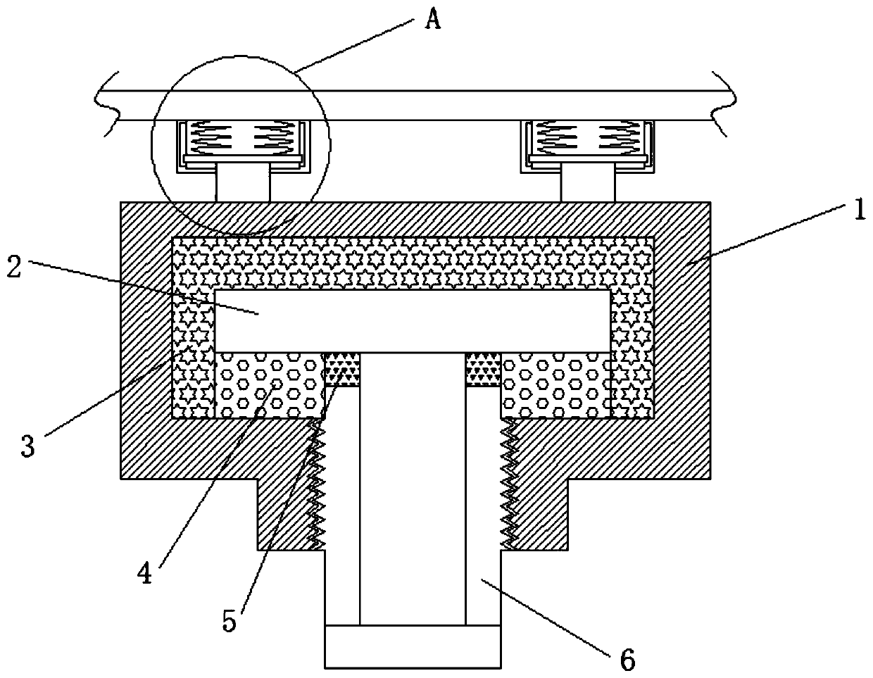
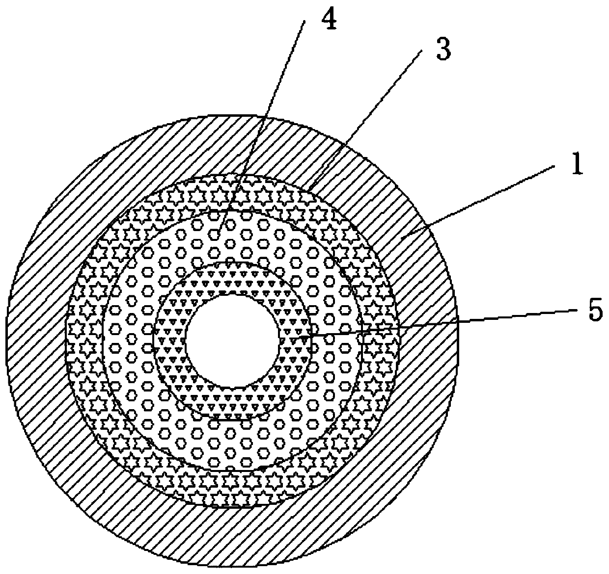
[0027] according to Figure 1-3 , the present invention proposes a packaging structure in which the front side of the sensor chip is exposed downward, including a base 1, a cavity is opened inside the base 1, a sensor chip body 2 is arranged inside the cavity, and a second sensor chip body 2 is arranged on the top of the base 1 A washer 3, the bottom inner wall of the base 1 is fixedly provided with a second washer 4, the inner wall of the second washer 4 is fixedly provided with a third washer 5, the bottom of the base 1 is penetrated with a screw rod 6, and the top of the base 1 is provided with There are two buffers.

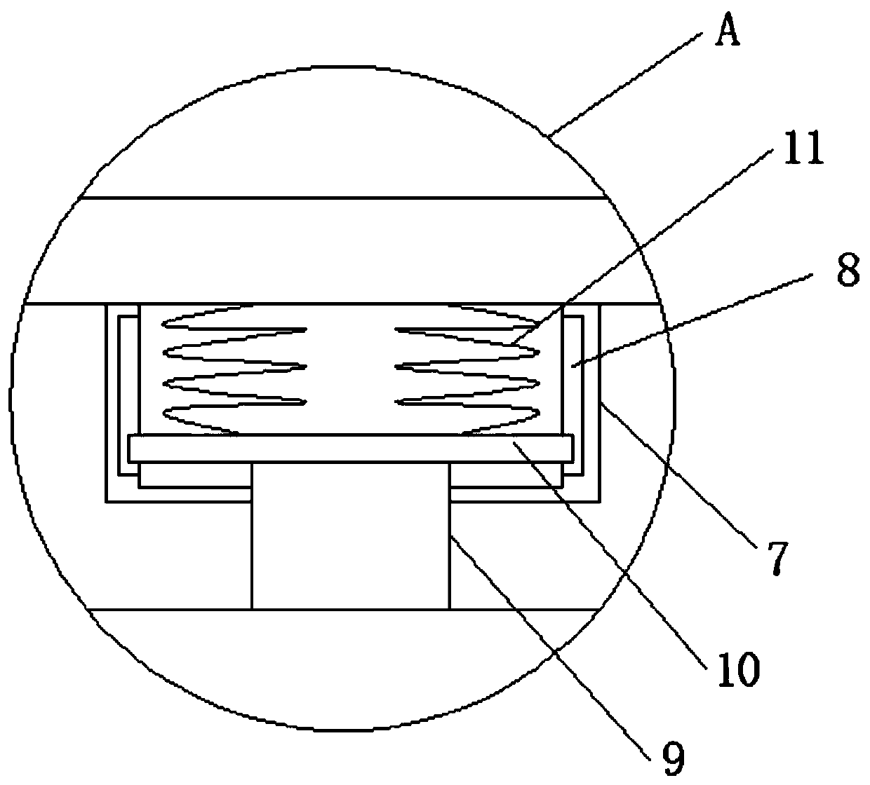
[0028] In this embodiment, the buffer device includes a fixed cover 7, a chute 8, a fixed rod 9, a slide rod 10 and a buffer spring 11. The inner walls of both sides of the fixed cover 7 are provided with chute 8, and the inner walls of the t...


PUM


Abstract

The invention discloses a packaging structure and a packaging method for downward exposure of the front surface of a sensor chip. The packaging structure comprises a base, wherein the base is internally provided with a cavity, the cavity is internally provided with a sensor chip body, the top of the base is provided with a first gasket, the bottom inner wall of the base is fixedly provided with asecond gasket, the inner wall of the second gasket is fixedly provided with a third gasket in a sleeving mode, a screw is arranged at the bottom of the base in a penetrating mode, and two buffer devices are arranged at the top of the base. The structure is simple and novel, the sealing function of the sensor chip is improved, the stability of the sensor is improved, the sensor is connected with the outside through a screw through hole, the use sensitivity is improved, and the packaging method is simple and suitable for market popularization.

Description

technical field [0001] The invention relates to the technical field of semiconductor packaging, in particular to a packaging structure and packaging method in which the front side of a sensor chip is exposed downward. Background technique [0002] In order to obtain information from the outside world, people must rely on sensory organs. People's own sensory organs are far from enough to study natural phenomena and laws and their functions in production activities. In the process of using information, the first thing to solve is to obtain accurate and reliable information, and sensors are the main ways and means to obtain information in the natural and production fields. In modern industrial production, especially in the automated production process, various sensors are used to monitor and control various parameters in the production process, so that the products can achieve the best quality. Therefore, it can be said that without a large number of excellent sensors, modern...

Claims


Application Information

Patent Timeline
Patent Type & Authority Applications(China)
IPC IPC(8): H01L23/04H01L23/10H01L23/31H01L21/52H01L21/56
CPCH01L23/04H01L23/10H01L23/3107H01L21/52H01L21/56
Inventor 尹亮亮楼夙训
Owner NINGBO ANCHUANG ELECTRONICS TECH CO LTD
Why Eureka
Try Eureka