Display device

A technology of a display device and a light-emitting unit, which is applied to the field of LED display devices, can solve the problems of complicated circuits related to the circuit board and high production cost of the circuit board, and achieves the effects of reducing the production cost, reducing the size, and increasing the setting density.

Pending Publication Date: 2020-03-03
BRIGHTEK (SHENZHEN) OPTOELECTRONIC CO LTD +1
View PDF0 Cites 2 Cited by
  • Summary
  • Abstract
  • Description
  • Claims
  • Application Information

AI Technical Summary

Problems solved by technology

[0004] The main purpose of the present invention is to provide a display device, which is used to improve the production cost of the circuit board of the existing high-density display device, and the related circuits of the circuit board are complicated.

Method used


Image

  • Display device
  • Display device
  • Display device

Examples


Embodiment Construction

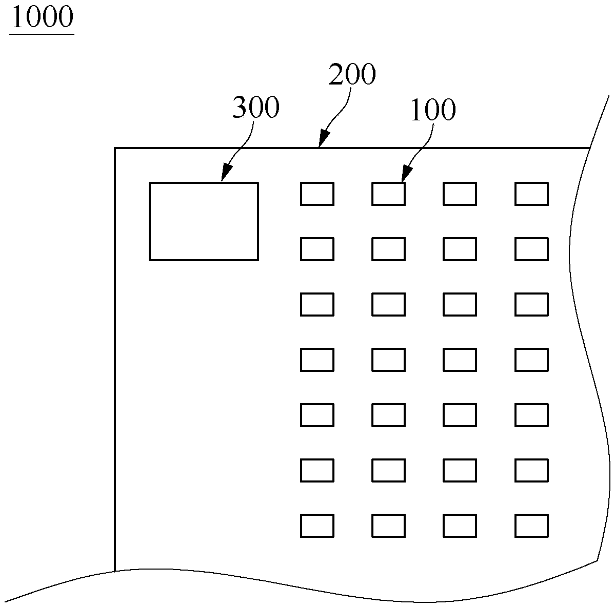
[0029] see figure 1 , which is a partial schematic diagram of the display device of the present invention. As shown in the figure, the display device 1000 includes: a plurality of light emitting units 100 , a circuit board 200 and a processing unit 300 . A plurality of light-emitting units 100 are arranged at intervals on the circuit board 200, the processing unit 300 is fixed on the circuit board 200, and the processing unit 300 can be electrically connected to each light-emitting unit 100 through the circuit board 200, and the processing unit 300 can independently control The brightness or color temperature of the light beams emitted by each light emitting unit 100 .

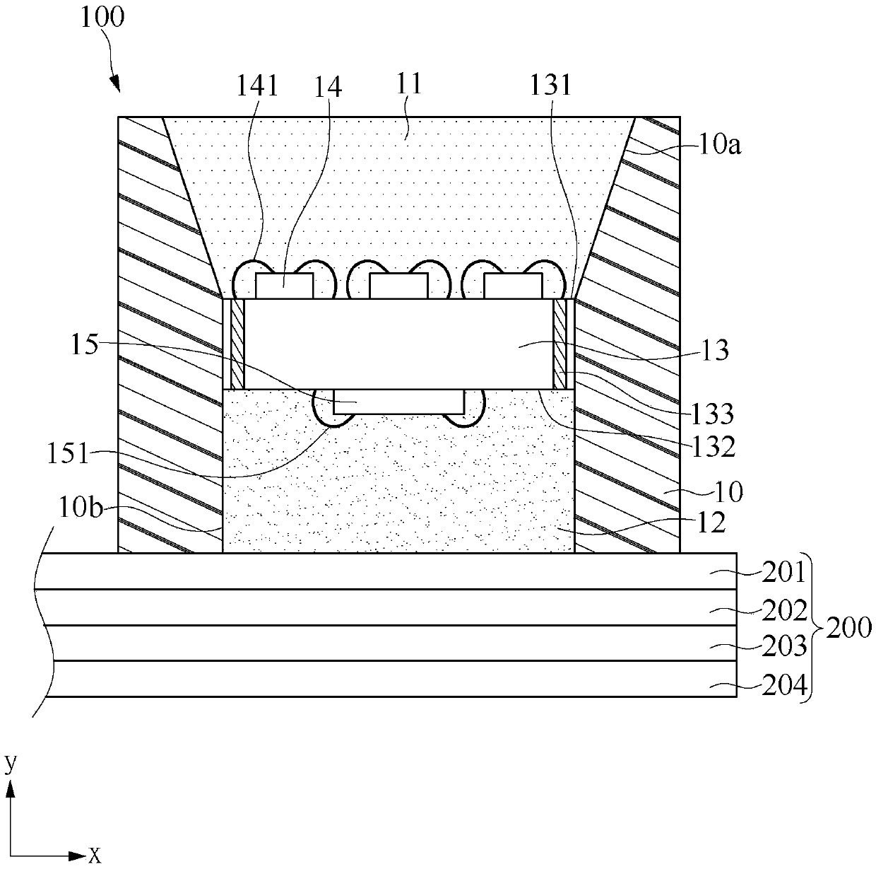
[0030] Such as figure 2 As shown, it is a schematic cross-sectional view of the circuit board 200 and a single light emitting unit 100 . The circuit board 200 may only include four electrical layer structures, which are a first signal layer structure 201 , a power layer structure 202 , a second signal laye...


PUM

PropertyMeasurementUnit
wavelengthaaaaaaaaaa

Abstract

The present disclosure relates to a display device. The display device comprises a plurality of light emitting units, a circuit mainboard and a processing unit. Each light emitting unit comprises an insulating body, a substrate, a light emitting chip, a driving chip and a pin. The two ends, opposite to each other, of the insulating body are respectively recessed to form a first groove and a secondgroove. The substrate is arranged in the insulating body. The light emitting chip is fixedly arranged on the substrate, and the light emitting chip is exposed out of the first groove. The driving chip is fixedly arranged on the substrate, and the driving chip is exposed out of the second groove. The first groove is filled with light-transmitting colloid. The second groove is filled with packagingcolloid. Each light emitting unit is fixedly arranged on the circuit mainboard. The processing unit is fixedly arranged on the circuit mainboard, the processing unit is electrically connected with the light emitting units, and the processing unit can control the brightness or color temperature of the light beams emitted by each light emitting unit independently. The display device in the invention can be used for solving the problems that the production cost of the circuit mainboard of the existing high-density display device is high and the related circuits of the circuit mainboard are complex.

Description

technical field [0001] The invention relates to a display device, especially a display device with high-density LEDs. Background technique [0002] Existing high-density display equipment is to arrange a plurality of LED units and related driving chips on a circuit board. Due to the huge number of LED units, the corresponding number of driving chips is also very large, thus having a circuit board. The circuit design is complicated and the production cost is high. [0003] In addition, in order to reduce the circuit complexity and production cost of the circuit board, some manufacturers will make a single driver chip drive multiple LED units at the same time. This design can slightly reduce the circuit complexity of the circuit board. When any one of the LED units jointly driven by the driver chip is damaged, multiple LED units may fail to operate together; or, when any driver chip is damaged, multiple LED units may fail to operate at the same time. Contents of the inventi...

Claims


Application Information

Patent Timeline
Patent Type & Authority Applications(China)
IPC IPC(8): G09F9/33
CPCG09F9/33
Inventor 黄建中李砚霆何俊杰
Owner BRIGHTEK (SHENZHEN) OPTOELECTRONIC CO LTD
Why Eureka
Try Eureka