Display panel and display device

A technology for display panels and driving backplanes, which is applied in the direction of electrical components, electric solid devices, circuits, etc., can solve the problems of micro LED falling off, and achieve the effect of solving the problem of loose binding and falling off, binding firmly, and improving adhesion

Inactive Publication Date: 2020-03-06
SHENZHEN CHINA STAR OPTOELECTRONICS SEMICON DISPLAY TECH CO LTD
View PDF11 Cites 8 Cited by
  • Summary
  • Abstract
  • Description
  • Claims
  • Application Information

AI Technical Summary

Problems solved by technology

[0006] This disclosure provides a display panel and a display device to alleviate the technical problem of the existing micro-LED falling off

Method used


Image

  • Display panel and display device
  • Display panel and display device
  • Display panel and display device

Examples


Embodiment Construction

[0026] The following descriptions of the various embodiments refer to the accompanying drawings to illustrate specific embodiments in which the present disclosure may be practiced. The directional terms mentioned in this disclosure, such as [top], [bottom], [front], [back], [left], [right], [inside], [outside], [side], etc., are for reference only The orientation of the attached schema. Therefore, the directional terms used are used to explain and understand the present disclosure, but not to limit the present disclosure. In the figures, structurally similar elements are denoted by the same reference numerals.

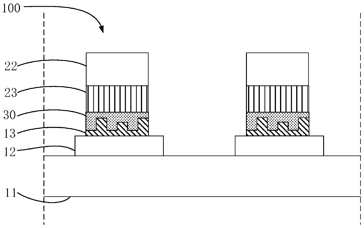
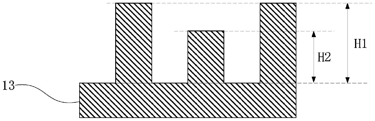
[0027] In one embodiment, as figure 1 As shown, a display panel 100 is provided, which includes a driving backplane 11 , a driving circuit 12 , a first electrode layer 13 , micro LEDs 22 , a second electrode layer 23 and a binding layer 30 . The driving circuit 12 is disposed on the driving backplane 11 . The first electrode layer 13 is disposed on the driving circ...


PUM


Abstract

The invention provides a display panel and a display device. The display panel comprises a driving backboard, a driving circuit, a first electrode layer, a micro LED, a second electrode layer and a binding layer. The first electrode layer on the driving circuit is provided with a first protruding structure, and the second electrode layer under the micro LED is provided with a second protruding structure. The binding layer is arranged between the first electrode layer and the second electrode layer. The contact area between the binding layer and the first electrode layer or the contact area between the binding layer and the second electrode layer is increased, so that the problem that the micro LED falls off is solved.

Description

technical field [0001] The present disclosure relates to the field of display technology, and in particular, to a display panel and a display device. Background technique [0002] Compared with the current LCD and OLED display devices, Micro-LED display devices have the advantages of fast response, high color gamut, high resolution, and low energy consumption. But its technical difficulties are many and complex, especially its key technology: mass transfer technology. [0003] Micro LED chips need to be transferred to the required positions one by one after the production is completed. The number of micro LED chips to be transferred is large and the position accuracy after transfer is high, which consumes a lot of resources. With the development of technology, mass transfer technology has developed many technical branches, such as electrostatic adsorption, laser burning and so on. [0004] Mass transfer technology is to bind a huge number of micro-LED chips to the drive ci...

Claims


Application Information

Patent Timeline
Patent Type & Authority Applications(China)
IPC IPC(8): H01L27/15
CPCH01L27/156H01L25/167H01L24/29H01L24/32H01L24/03H01L24/05H01L2224/0362H01L2224/03622H01L2224/05557H01L2224/05573H01L2224/05611H01L2224/29019H01L2224/29109H01L2224/29111H01L2224/32145H01L2924/12041
Inventor 胡小波
Owner SHENZHEN CHINA STAR OPTOELECTRONICS SEMICON DISPLAY TECH CO LTD
Why Eureka
Try Eureka