Transparent COF design method
A design method and transparent technology, applied in the field of COF, can solve problems such as poor line detection, inability to see COF lines, and affect product quality, and achieve the effects of improving product quality, high flexibility, and improving accuracy
- Summary
- Abstract
- Description
- Claims
- Application Information
AI Technical Summary
Problems solved by technology
Method used
Image
Examples
Embodiment
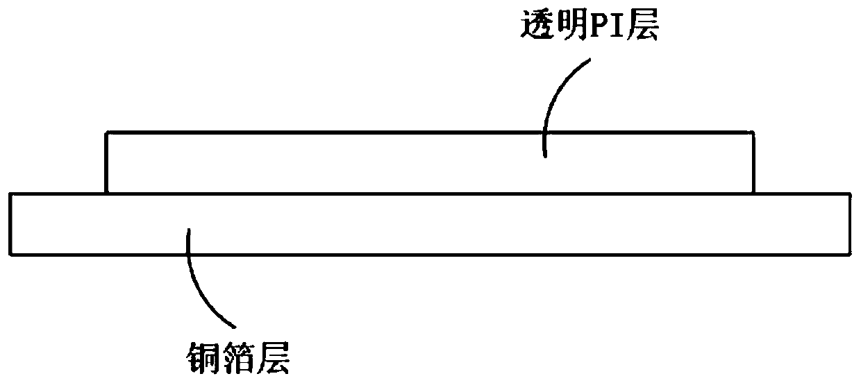
[0021] Such as figure 1 As shown, the embodiment of the present invention provides a transparent COF design method, the transparent COF is composed of a transparent PI layer and a copper foil layer;
[0022] The transparent COF includes the following preparation steps:
[0023] S1. Prepare a transparent PI layer, check the used transparent PI layer, and confirm that the transparent PI layer is not damaged, and the thickness of the transparent PI layer is 5 μm to 100 μm;
[0024] S2. Form the main copper foil layer on one side of the transparent PI layer by electroless copper plating, the thickness of the copper foil layer is 3 μm to 30 μm, and the transparent COF can be obtained;
[0025] S3. Detecting the prepared transparent COF to determine whether various properties of the transparent COF are qualified.
[0026] By using the transparent COF composed of transparent PI layer and copper foil layer, the internal circuit status can be clearly seen, which improves the accuracy...
PUM
| Property | Measurement | Unit |
|---|---|---|
| thickness | aaaaa | aaaaa |
| thickness | aaaaa | aaaaa |
Abstract
Description
Claims
Application Information
