Custom lead frame from standard plus printed lead frame portion

A technology of metal leads and metal traces, which is applied in semiconductor/solid-state device manufacturing, semiconductor/solid-state device components, semiconductor devices, etc., can solve the problems of time-consuming, high LF design cost, etc., and achieve the effect of reducing quantity

Pending Publication Date: 2020-03-13
TEXAS INSTR INC
0 Cites 1 Cited by

AI-Extracted Technical Summary

Problems solved by technology

LF is usually designed together with IC die in a co-design process, the design includes mechan...

Method used

[0014] The custom LF 100 includes a dielectric support surface 131 in the gap between the metal structures of the standard LF part 110, which provides mechanical support for the printed LF part 120 beyond the area of ​​the standard LF. The dielectric support surface 131 may be provided as a surface of a support 130, which typically includes a pre-molded structure in which the leads 110b are embedded leads with exposed top surfaces such that there is a dielectric material between adjacent leads 110b. The pre-molded structure may comprise a pre-molded standard LF providing a standard LF portion 110, wherein the molding compound provides the dielectric support surface 131 and the leads 110b are exposed, or interconnected by single or multi-level molding comprising a pre-molded structure Substrate (MIS), the pre-molded structure includes a MIS lead frame providing a standard LF part 110, where the top dielectric layer of the MIS serves as a dielectric support surface 131 and the leads 110b are exposed. The standard LF part 110 can also be p...

Abstract

The invention discloses a custom lead frame from a standard plus printed lead frame portion, and discloses a packaged semiconductor device (200). The packaged semiconductor device (200) includes an ICdie (140) having bump (140a) features that are coupled to bond pads (140) flip chip attached to a custom LF (140). The custom LF includes metal structures including metal leads (110b) on at least twosides, and printed metal providing a printed LF portion including printed metal traces (120a) that connect to and extend inward from at least one of the metal leads over the dielectric support material that are coupled to FC pads (120b) configured for receiving the bump features including at least some of the printed metal traces (120a) coupled to the bond pads on the IC die. The IC die (120b) isflip chip mounted on the printed LF portion so that the bump features are connected to the FC pads.

Application Domain

Semiconductor/solid-state device detailsSolid-state devices +2

Technology Topic

Mechanical engineeringDevice material +3

Image

  • Custom lead frame from standard plus printed lead frame portion
  • Custom lead frame from standard plus printed lead frame portion
  • Custom lead frame from standard plus printed lead frame portion

Examples

  • Experimental program(1)

Example Embodiment

[0012] Example embodiments are described with reference to the accompanying drawings, where the same reference numerals are used to indicate similar or equivalent elements. The graphical ordering of actions or events should not be regarded as a limitation, as certain actions or events can occur in a different order and/or simultaneously with other actions or events. In addition, some of the illustrated actions or events may not be required to implement the method according to the present disclosure.
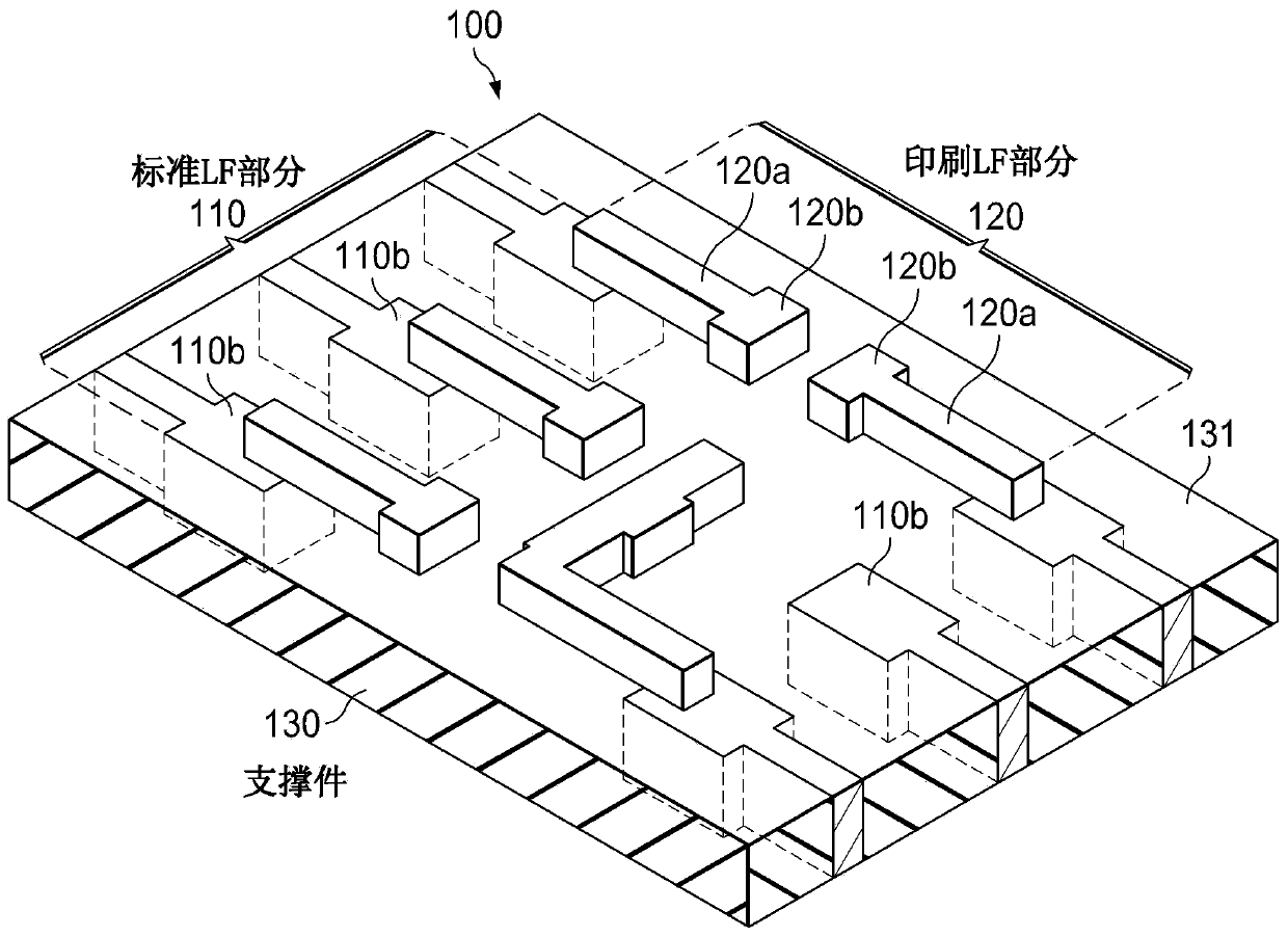
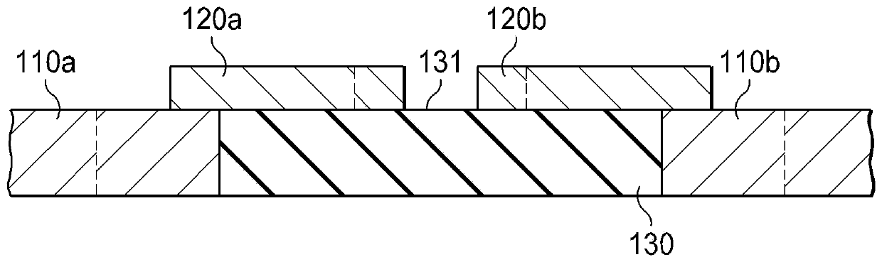
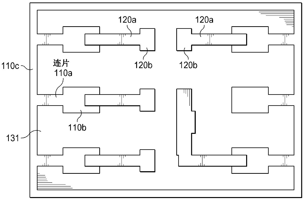
[0013] figure 1 A simplified example customized LF 100 according to an example embodiment is shown, which shows its standard LF part 110 with leads 110b on at least two sides, and a printed LF part 120 coupled to the leads 110b of the standard LF part 110. There is usually some design overlap between the trace 120a and the lead 110b of the printed LF portion 120 to reflect manufacturing tolerances to ensure reliable connection. The custom LF 100 is generally part of a custom LF strip that includes multiple LFs. The printed metal may have a porosity greater than 10%.
[0014] The customized LF 100 includes a dielectric support surface 131 in the gap between the metal structures of the standard LF portion 110, which provides mechanical support for the printed LF portion 120 beyond the area of ​​the standard LF. The dielectric support surface 131 may be provided as the surface of the support 130, which generally includes a pre-molded structure, where the lead 110b is an embedded lead with an exposed top surface such that there is a dielectric material between adjacent leads 110b. The pre-molded structure may include a pre-molded standard LF that provides a standard LF portion 110, where the molding compound provides the dielectric support surface 131 and the leads 110b are exposed, or interconnected by single-stage or multi-stage molding including the pre-molded structure Substrate (MIS), this pre-molded structure includes a MIS lead frame providing a standard LF part 110, where the top dielectric layer of the MIS serves as the dielectric support surface 131 and the leads 110b are exposed. The standard LF portion 110 may also be provided or treated to have a nano-rough surface to improve the adhesion of the trace 120a of the printed LF portion 120 and the lead 110b.
[0015] The printed LF is formed by additive deposition (for example, 3D printing, i.e. inkjet printing, or screen printing) of a metal precursor (for example, an ink or paste comprising a plurality of metal particles) to form a printed metal precursor in a usual/substantially deposited printing LF Part 120. Sintering or curing is usually performed after additive deposition to form a printed LF portion 120 including FC pad 120b and metal trace 120a, which is connected to at least one metal lead 110b and inwardly from above dielectric support surface 131 extend. The typical thickness of the printed metal precursor is 75 μm to 150 μm. The additive deposition process can include multiple coating and sintering steps, such as a series of powder coating followed by laser exposure.
[0016] For some devices, some traces 120a may extend from one side of the custom LF 100 without any FC bonding pad 120b in the path, for example to provide a common ground or heat dissipation path. The IC die is then flip-chip coupled to FC pad 120b, which is configured to receive bump features, which are coupled to bond pads on the IC die to be mounted. The sintering or curing of the metal precursor is usually performed before flip-chip mounting. The FC pad 120b is positioned for flip-chip mounting of the IC die on the printed metal so that the bump features (see the description below Figure 2C The bump feature 140a) in) falls on the FC pad 120b. After the IC die is flip-chip mounted, the LF strip is usually heated to a temperature higher than the melting point of the solder material used in a conventional solder reflow process, which can improve the conductivity of the printed LF portion 120.
[0017] As is known in the printing field, inks include solid (eg, particles, such as nanoparticles) materials or materials for solid precursors, which include solvents and/or dispersions after curing or sintering to remove them. The liquid carrier of the agent then forms a solid (e.g., granules). For example, the ink may be a sinterable metallic ink or an ultraviolet (UV) curable polymer or a UV curable polymer-based mixture. Ink can be additively deposited through the printer platform to its programmed desired location. The ink deposition device may be an inkjet printer, an electrostatic inkjet printer, or a screen or flexographic printer using piezoelectric, thermal, or acoustic.
[0018] The metal paste can be processed, for example, after additive deposition by screen printing, the processing includes a heating step in a reducing gas atmosphere, followed by a vacuum sintering step usually performed at a temperature of at least 200°C to form a sintered Metal coating. The metal slurry can be conventionally sintered in a curing oven to remove the binder and solvent (if present), and be densified to reduce the porosity of the metal material.
[0019] Figure 2A-Figure 2F A view showing various stages of assembling a packaged semiconductor device including a disclosed custom lead frame including a standard LF part and a printed LF part. Figure 2A Shows a side view of the standard LF part after additive deposition printing of the LF part, and Figure 2B Shows its top view, the standard LF part is shown by its lead 110b and connecting piece 110a, and the printed LF part is shown by its metal trace 120a and FC pad 120b supported by a dielectric supporting surface 131 which is Located in the gap between the metal structures of the standard LF section. The tab 110a fixes the metal lead 110b to the frame 110c. Figure 2C Shows a side view of the standard LF after flip-chip mounting the IC die 140, and Figure 2D Shows its top view, the standard LF is shown by its lead 110b and connecting piece 110a, the IC die 140 has a bonding pad 140b, wherein the bump feature 140a on the bonding pad 140b is on the printed LF part, so that The bump feature 140a of the IC die falls on the FC pad 120b of the printed LF portion.
[0020] Figure 2E A side view after molding to form the molding material 150 surrounding the LF sheet is shown. Figure 2F A side view after singulation of the molded LF sheet to form the packaged semiconductor device 200 shown is shown.
[0021] Figure 3A Shows a top view of the standard LF part with floating lead 110d, and Figure 3B After printing the printed LF portion 120' contacting the other leads of the standard LF Figure 3A The standard LF part in. Floating leads can increase IC package input/output (I/O) configuration flexibility and heat dissipation by providing exposed pads on the backside of the package near the middle of the IC, and reduce mechanical stress. Floating lead designs are some commercially available existing packages (e.g. HOTROD of Texas Instruments for various power converter devices) TM Package) standard features.
[0022] The method of forming the disclosed custom LF can first determine a number of preliminary candidate LF designs that also meet the device requirements of the IC die, including the number of I/Os, voltage and/or current ratings, and mechanical and/or Thermal Stress. The number of preliminary candidate LFs can be reduced to identify candidate LFs by simulating preliminary candidate LFs to quantify its device performance. This reduction process creates a set of candidate LF designs that meet all the requirements of a particular IC device. Repeat the same process for other IC devices that have different voltage and/or current ratings and mechanical and/or thermal stresses but somewhat similar I/O numbers and package sizes. This process step creates a set of candidate custom LF designs for different IC devices with similar numbers of I/O and die sizes.
[0023] Generally, one or more standard LFs will be designed based on common features shared by two or more candidate LFs. The algorithm can identify common features in candidate custom LF designs, which together determine the standard LF design. The standard design LF is then manufactured into LF strips using conventional LF manufacturing technology. A 3D printing technique is then used to manufacture a printed metal part that includes a printed trace that extends to the contacts on top of the edge of the standard LF trace to replicate the candidate LF design. In this way, standard LF designs can be used for candidate LF designs for different devices.
[0024] Depending on how the candidate LF designs are classified, there can be more than one standard LF design. Candidate LF designs can be classified based on similarity, such as the number of I/Os, package size, heat dissipation performance, and mechanical strength.
[0025] As described above, the surface of the LF 110 may include nano-roughening. Next, the metal precursor material is additively deposited, and then sintered or cured (for example, laser treatment) to provide metal traces and FC pads, and connect the metal traces to the leads of standard LF for the desired Routing and used to meet other LF properties, such as the number of I/O pins, heat dissipation, and mechanical stress. Additive deposition can include inkjet printing using piezoelectric, thermal, or acoustic, or electrostatic inkjet printing, screen printing, or flexographic printing. Molding and singulation of LF strips is usually at the back.
[0026] The printing metal precursor material may include an ink that contains a solid material or a material for a solid precursor, which forms a solid after being cured or sintered. The ink includes copper or silver nanoparticles. Generally, the printed metal has a porosity greater than that of the metal of the LF, the mechanical strength is less than that of the metal of the LF, and the conductivity is less than that of the metal of the LF.
[0027] There are several standard LF options that can be used with the disclosed aspects. Two or more standard LFs can be combined, such as a top lead frame on a bottom lead frame. Some leads of standard LF can also be floating, as described above Figure 3A with 3B As shown, this can add more flexibility to the IC package I/O configuration, such as heat dissipation and/or provide mechanical stress relief.
[0028] The advantages provided by the disclosed custom LF include reducing the time and cost of LF orders, standardizing LF design and IC bump design to reduce the number of masks required. In addition, the additive manufacturing of the metal layer allows flexible design and manufacturing of LF.
[0029] The disclosed embodiments can be integrated into various assembly processes to form various semiconductor integrated circuit (IC) devices and related products. The assembly may include a single semiconductor die or multiple semiconductor dies, such as a PoP configuration including multiple stacked semiconductor dies. Various package substrates can be used. The semiconductor die may include various elements therein and/or various layers thereon, including barrier layers, dielectric layers, device structures, active elements, and passive elements, including source regions, drain regions, and bit lines , Base, emitter, collector, conductive wire, conductive via, etc. In addition, semiconductor dies can be formed by a variety of processes, including bipolar transistors, insulated gate bipolar transistors (IGBT), CMOS, BiCMOS, and MEMS.
[0030] Those skilled in the art to which the present disclosure relates will understand that within the scope of the claimed invention, many other embodiments and variations of the embodiments are possible, and without departing from the scope of the present disclosure, the described The embodiments are further added, deleted, replaced and modified.

PUM

no PUM

Description & Claims & Application Information

We can also present the details of the Description, Claims and Application information to help users get a comprehensive understanding of the technical details of the patent, such as background art, summary of invention, brief description of drawings, description of embodiments, and other original content. On the other hand, users can also determine the specific scope of protection of the technology through the list of claims; as well as understand the changes in the life cycle of the technology with the presentation of the patent timeline. Login to view more.

Similar technology patents

Ion thruster beam test method based on Faraday probe array

ActiveCN105116435ALarge amount of data informationreduce in quantity
Owner:LANZHOU INST OF PHYSICS CHINESE ACADEMY OF SPACE TECH

Classification and recommendation of technical efficacy words

Why Eureka
Try Eureka