Magnetic memory and write state detection method thereof

A technology of magnetic memory and writing state, which is applied in the field of semiconductor chips, can solve problems such as chip errors and low tolerance, and achieve the effect of avoiding misjudgment and saving power consumption

Active Publication Date: 2020-03-17
SHANGHAI CIYU INFORMATION TECH
View PDF10 Cites 0 Cited by
  • Summary
  • Abstract
  • Description
  • Claims
  • Application Information

AI Technical Summary

Problems solved by technology

(4) Unlike DRAM and Flash, MRAM is not compatible with standard CMOS semiconductor processes. MRAM can be integrated into a chip with logic circuits
[0018] 2. Need a reference unit with a reference resistor
[0024] 2. If the memory cells in the chip are used to construct a reference cell, in the architecture of a single reference cell, the resistance of this reference cell must be in the P state (parallel magnetization direction, corresponding to low resistance state) and AP state (antiparallel magnetization direction, corresponding to High resistance state) A certain value between the average resistance can only be averaged in parallel with a set of reference cells in the P state and a set of reference cells in the AP state, such as most reading circuits
Due to various deviations in the chip including measurement errors, some units that have not completed the write operation are misjudged as write operations, which will cause chip errors. For a memory chip, the tolerance for errors is very, very low

Method used


Image

  • Magnetic memory and write state detection method thereof
  • Magnetic memory and write state detection method thereof
  • Magnetic memory and write state detection method thereof

Examples


Embodiment Construction

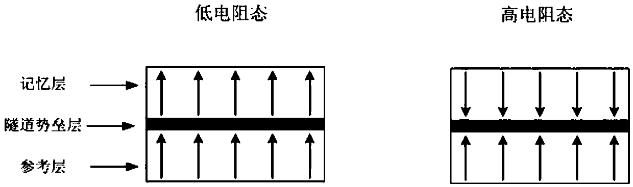
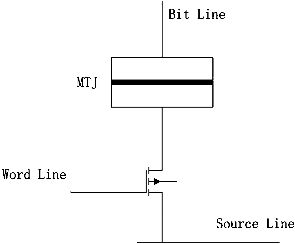
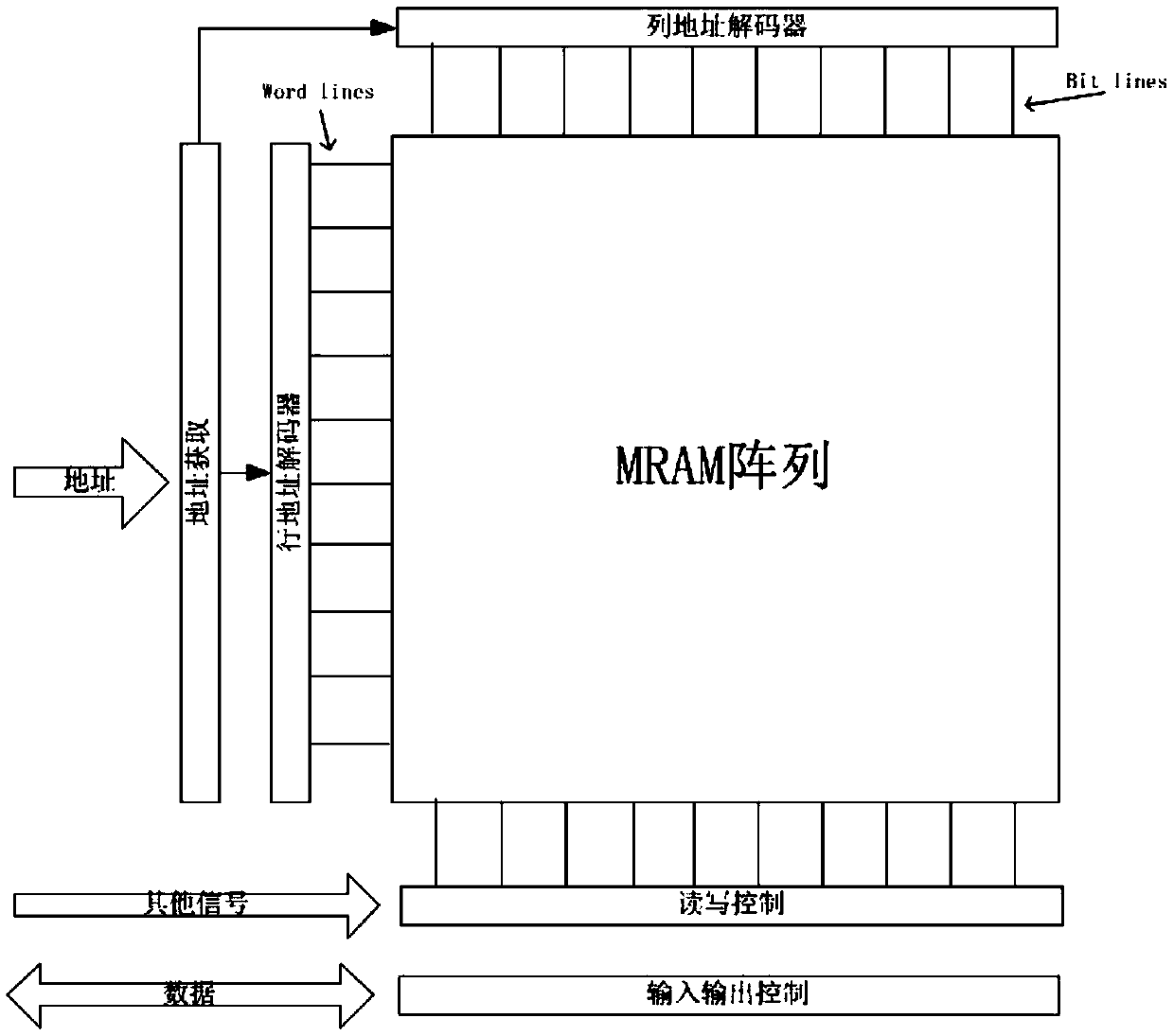
[0059] In describing the embodiments of the present invention, it should be understood that the terms "upper", "lower", "front", "rear", "left", "right", "vertical", "horizontal", "top ", "Bottom", "Inner", "Outer", "Clockwise", "Counterclockwise" and other indicated orientations or positional relationships are based on the orientations or positional relationships shown in the drawings, and are only for the convenience of describing the present invention and Simplified descriptions, rather than indicating or implying that the device or element referred to must have a particular orientation, be constructed and operate in a particular orientation, and thus should not be construed as limiting the invention. The attached drawings are schematic diagrams or conceptual diagrams, and the relationship between the thickness and width of each part, as well as the proportional relationship between each part, etc., are not completely consistent with their actual values.

[0060] The presen...


PUM


Abstract

The invention provides a magnetic memory and a write state detection method thereof, and the magnetic memory comprises a high-resistance state write reference unit which is used for providing a reference signal for judging whether a storage unit is in a high-resistance state or not; a low-resistance state write reference unit used for providing a reference signal for judging whether the storage unit is in a low-resistance state or not; and a write-in state detection unit used for receiving output signals of the high-resistance state write reference unit and the low-resistance state write reference unit and corresponding detection signals in write-in loops of the storage units. When writing operation set to be in a high-resistance state is carried out, the writing state detection unit compares a detection signal of the storage unit with a signal provided by the high-resistance state writing reference unit, and when it is judged that the storage unit is in the high-resistance state, awriting stopping signal is sent out; when writing operation set to be in a low-resistance state is carried out, the writing state detection unit compares a detection signal of the storage unit with asignal provided by the low-resistance state writing reference unit, and when it is judged that the storage unit is in the low-resistance state, a writing stopping signal is sent out.

Description

technical field [0001] The invention relates to the field of semiconductor chips, and its most important application lies in the fields of the Internet of Things and wearable electronic devices that have strict requirements on standby power consumption, and in particular relates to a magnetic memory and a write state detection method thereof. Background technique [0002] In recent years, people have made use of the magnetoresistance effect of a magnetic tunnel junction (MTJ, Magnetic Tunnel Junction) to make a magnetic random access memory, which is MRAM (Magnetic Random Access Memory). MRAM is considered to be the future solid-state non-volatile memory, which has the characteristics of high-speed reading and writing, large capacity and low energy consumption. Compared with existing memory, its advantages include: (1) It has the high-speed read and write capability of static random access memory (SRAM), and the high integration of dynamic random access memory (DRAM), and it...

Claims


Application Information

Patent Timeline
IPC IPC(8): G11C11/16
CPCG11C11/161G11C11/1673G11C11/1675
Inventor 戴瑾叶力夏文斌
Owner SHANGHAI CIYU INFORMATION TECH
Why Eureka
Try Eureka