Lifting thimble assembly, electrostatic chuck and processing device with electrostatic chuck

A technology of electrostatic chuck and thimble, which is applied in the direction of circuits, discharge tubes, electrical components, etc., and can solve the problems of cooling gas discharge phenomenon, threatening the working stability and safety of electrostatic chucks, etc.

Active Publication Date: 2020-03-20
ADVANCED MICRO FAB EQUIP INC CHINA
View PDF8 Cites 5 Cited by
  • Summary
  • Abstract
  • Description
  • Claims
  • Application Information

AI Technical Summary

Problems solved by technology

[0005] With the increase of the RF power applied to the reaction chamber, this cooling technology is likely to cause the cooling gas to discharge in the channel containing the lifting thimble, which ser...

Method used


Image

  • Lifting thimble assembly, electrostatic chuck and processing device with electrostatic chuck
  • Lifting thimble assembly, electrostatic chuck and processing device with electrostatic chuck
  • Lifting thimble assembly, electrostatic chuck and processing device with electrostatic chuck

Examples


Embodiment Construction

[0036] In order to make the purpose, technical solutions and advantages of the embodiments of the present invention clearer, the technical solutions in the embodiments of the present invention will be clearly and completely described below in conjunction with the drawings in the embodiments of the present invention. Obviously, the described embodiments It is a part of embodiments of the present invention, but not all embodiments. Based on the embodiments of the present invention, all other embodiments obtained by persons of ordinary skill in the art without making creative efforts belong to the protection scope of the present invention.

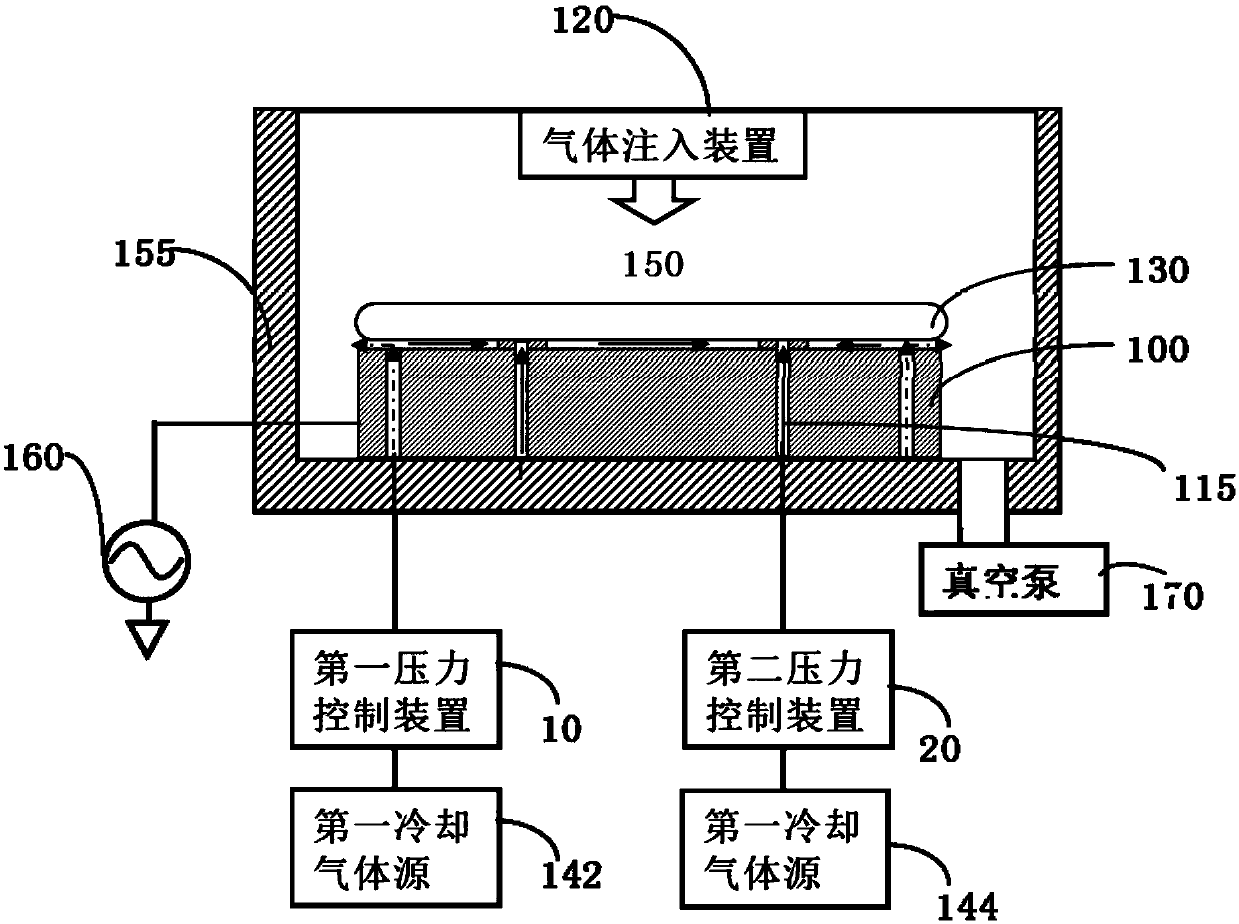
[0037] figure 1 A plasma processing apparatus is shown, comprising an evacuatable reaction chamber 150 surrounded by an outer wall 155 . The reaction chamber 150 is used for processing the substrate. An electrostatic chuck 100 is disposed at the bottom of the reaction chamber for supporting and fixing the substrate 130 . A gas injection de...


PUM


Abstract

The invention discloses a lifting ejector pin assembly, an electrostatic chuck provided with the lifting ejector pin assembly and a processing device where the electrostatic chuck is located. The lifting ejector pin assembly comprises a lifting ejector pin. The channel is used for accommodating the lifting thimble; the channel for accommodating the lifting thimble is connected with a pressure control device; a sealing ring is arranged at one end, close to the substrate, of the channel for accommodating the lifting thimble; the upper surface of the sealing ring is in contact with the back surface of the substrate in the technological process, so that gas on the back surface of the substrate is prevented from entering the channel for accommodating the lifting ejector pin, and the pressure control device can independently control the pressure in the channel for accommodating the lifting ejector pin.

Description

technical field [0001] The invention relates to the technical field of plasma etching, in particular to the technical field of plasma processing for preventing arc generation in an electrostatic chuck under high radio frequency power. Background technique [0002] Micromachining of semiconductor substrates or substrates is a well-known technique that can be used to fabricate, for example, semiconductors, flat panel displays, light emitting diodes (LEDs), solar cells, and the like. An important step in micromachining manufacturing is the plasma treatment process step, which is carried out inside a reaction chamber into which process gases are fed. A radio frequency source is inductively and / or capacitively coupled to the interior of the reaction chamber to energize the process gas to form and maintain a plasma. Inside the reaction chamber, the exposed substrate is supported by an electrostatic chuck and fixed in a fixed position by a certain clamping force to ensure the safe...

Claims


Application Information

Patent Timeline
IPC IPC(8): H01L21/683H01L21/687H01J37/32H01J37/20
CPCH01L21/6833H01L21/68742H01J37/32715H01J37/20H01J37/32513H01J37/32724H01J37/32816H01L21/6831H01L21/67109H01L21/67126H01L21/67253H01L21/67069H01L21/68721H01L21/67242H01L21/67098H01L21/3065H01J37/32174H01L21/67028H01L21/67248
Inventor 倪图强叶如彬黄国民梁洁涂乐义吴紫阳
Owner ADVANCED MICRO FAB EQUIP INC CHINA
Why Eureka
Try Eureka