
Miniature electronic component positioning and laminating device and method

A technology for electronic components and bonding devices, which is applied in the direction of electrical components, electric solid devices, circuits, etc., can solve problems such as troublesome bonding, high difficulty, and small size, so as to improve production efficiency and yield, solve difficult picking, and reduce effect of difficulty

Active Publication Date: 2020-03-24
东莞普莱信智能技术有限公司
View PDF15 Cites 4 Cited by
  • Summary
  • Abstract
  • Description
  • Claims
  • Application Information

AI Technical Summary

Problems solved by technology

However, according to experience, LEDs below 0.1mm are difficult to be picked up by vacuum nozzles due to the size relationship, so in the process of preparing Mini / Micro LED display panels using the preparation process provided by related technologies, the process of laminating Mini / Micro LED It is cumbersome, which leads to complicated manufacturing process of Mini / Micro LED display panels and low manufacturing efficiency. At the same time, due to the small size of Mini / Micro LEDs, it brings trouble to attach one by one
[0004] First of all, because the size of Mini LED or Micro LED is quite small, using the traditional form of attaching them one by one with a suction nozzle, the requirements for the suction holes on the suction nozzle are too high
At the same time, it is very difficult for the suction nozzle to pick up the Mini / Micor LED, and the success rate is not high.
In addition, in the traditional method, it is necessary to align first, then the suction nozzle picks up, and then moves to the designated position, and then the suction nozzle places the LED, resulting in low bonding efficiency

Method used


Image

  • Miniature electronic component positioning and laminating device and method
  • Miniature electronic component positioning and laminating device and method
  • Miniature electronic component positioning and laminating device and method

Examples


Embodiment Construction

[0040] In order to make the purpose, technical solutions and advantages of the embodiments of the present invention clearer, the technical solutions in the embodiments of the present invention will be clearly and completely described below in conjunction with the drawings in the embodiments of the present invention. Obviously, the described embodiments It is a part of embodiments of the present invention, but not all embodiments. Based on the embodiments of the present invention, all other embodiments obtained by persons of ordinary skill in the art without creative efforts fall within the protection scope of the present invention.

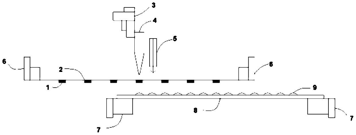
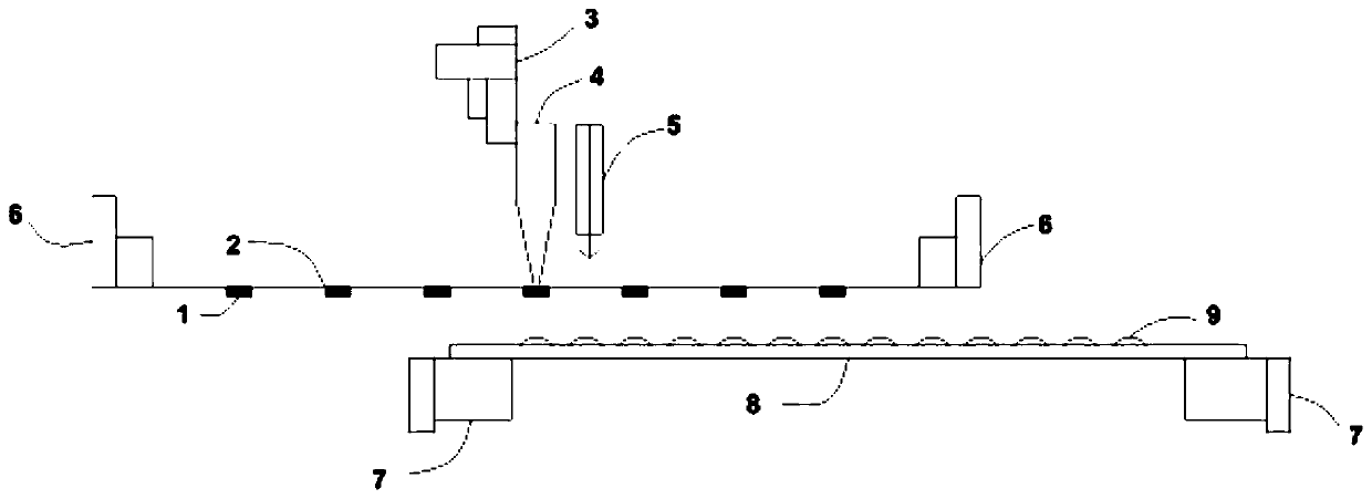
[0041] Please refer to figure 1 , the embodiment of the present invention provides a microelectronic component positioning and adhering device, including a first carrier tray 2, a micro thimble 4, a thimble drive mechanism 3, a first carrier tray drive mechanism 6, and a second carrier tray 8 and the camera 5, the various components of this embod...


PUM


Abstract

The invention discloses a miniature electronic component positioning and laminating device and a method thereof. The device comprises a first sticky object carrying disc, a first object carrying discdriving mechanism, a miniature ejector pin, an ejector pin driving mechanism, a second sticky object carrying disc and a camera, the adsorption force of the first carrying disc to the micro electroniccomponent is smaller than that of the second carrying disc. According to the invention, miniature electronic components on the first object carrying disc can be directly poked to a designated position on the second object carrying disc through the miniature thimbles for fitting; then curing welding is carried out in a backflow mode and the like; the process that the suction nozzles suck one by one and move back and forth to attach the single micro electronic component is omitted in the process; according to the invention, the production efficiency and the yield are improved, the method is especially suitable for positioning and fitting of Mini / Micro LEDs in the production process of Mini / Micro LED panels, the positioning and fitting process is simplified, the positioning and fitting difficulty is reduced, and a low-cost solution is provided for large-scale production.

Description

technical field [0001] The invention relates to the technical field of microelectronic component processing equipment, and more specifically, relates to a microelectronic component positioning and bonding device and method thereof. Background technique [0002] With the advancement of technology, more and more electronic components are developing towards miniaturization, such as LED. In the production process of LED panels, bonding equipment is usually used to pick up the LEDs one by one and paste them on the array substrate according to certain position requirements, and solder the LEDs to the array substrate through the chip-level welding (Chip bonding) process , and finally prepare an LED display panel. The display panel includes an array substrate and a plurality of LEDs arrayed on the array substrate, and each LED can be regarded as a pixel. With the development of display technology, the display is required to be more delicate. For the same size, more and more pixels...

Claims


Application Information

Patent Timeline
Patent Type & Authority Applications(China)
IPC IPC(8): H01L21/683H01L21/67H01L33/48
CPCH01L21/67144H01L21/6835H01L33/48H01L2221/68372H01L2221/68381
Inventor 田兴银毛军
Owner 东莞普莱信智能技术有限公司
Learn More