Semiconductor device and forming method thereof

A semiconductor and device technology, applied in the field of semiconductor devices and their formation, can solve problems such as reducing the channel leakage current of transistors with buried gate structures, and achieve the effect of reducing the channel leakage current

Pending Publication Date: 2020-03-24
CHANGXIN MEMORY TECH INC
View PDF0 Cites 3 Cited by
  • Summary
  • Abstract
  • Description
  • Claims
  • Application Information

AI Technical Summary

Problems solved by technology

[0002] Dynamic random access memory (DRAM) usually uses transistors with buried gate structure, but at present, in the manufacturing process of DRAM, there is no method that can effectively reduce the channel leakage current of transistors with buried gate structure

Method used


Image

  • Semiconductor device and forming method thereof
  • Semiconductor device and forming method thereof
  • Semiconductor device and forming method thereof

Examples


Embodiment Construction

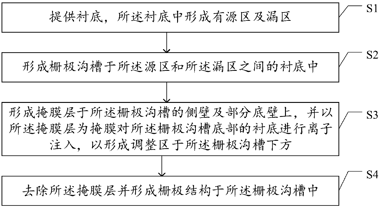
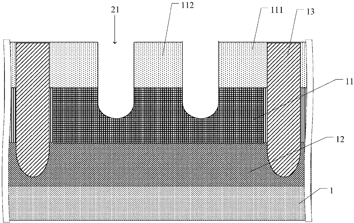
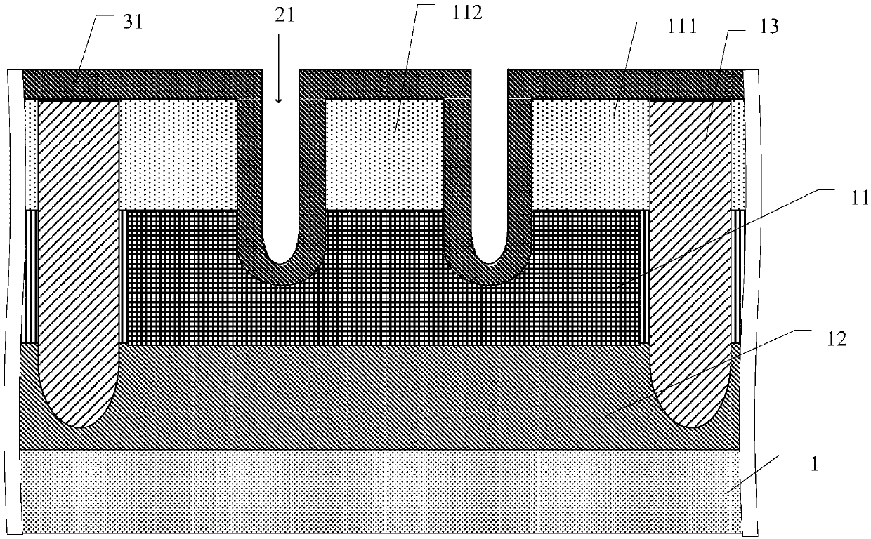
[0042] The specific implementation manner of the present invention will be described in more detail below with reference to schematic diagrams. Advantages and features of the present invention will be apparent from the following description and claims. It should be noted that all the drawings are in a very simplified form and use imprecise scales, and are only used to facilitate and clearly assist the purpose of illustrating the embodiments of the present invention.

[0043] Figure 6 The schematic diagram of the semiconductor device provided for this embodiment, such as Figure 6 As shown, the semiconductor device includes: a substrate 1 in which an active region 111 and a drain region 112 are formed; a gate structure 2 formed between the source region 111 and the drain region 112 A transistor is formed in the substrate 1 ; and an adjustment region 113 is located in the substrate 1 under the gate structure 2 to increase the doping concentration of the channel of the transis...


PUM

PropertyMeasurementUnit
Thicknessaaaaaaaaaa
Thicknessaaaaaaaaaa

Abstract

The invention provides a semiconductor device and a forming method thereof. A gate structure is formed between a source region and a drain region in the substrate to form a transistor, an adjustment region is formed at the bottom of the gate structure; a potential barrier is formed in a channel by increasing the doping concentration of the channel of the transistor, so that leakage current is prevented from passing through the channel, the leakage current of the channel is further reduced, meanwhile, due to the fact that the potential barrier is not very high, the potential barrier can be crossed by applying a low voltage to a gate structure, and other electrical characteristics of a semiconductor device are basically not affected.

Description

technical field [0001] The invention relates to the technical field of semiconductor manufacturing, in particular to a semiconductor device and a forming method thereof. Background technique [0002] A dynamic random access memory (DRAM) usually adopts a transistor with a buried gate structure, but at present, in the manufacturing process of the DRAM, there is no method that can effectively reduce the channel leakage current of the transistor with a buried gate structure. Contents of the invention [0003] The object of the present invention is to provide a semiconductor device and its forming method, which can conveniently and effectively reduce the channel leakage current of the transistor without affecting other electrical characteristics of the semiconductor device. [0004] In order to achieve the above object, the present invention provides a semiconductor device, comprising: [0005] a substrate in which an active region and a drain region are formed; [0006] a g...

Claims


Application Information

Patent Timeline
IPC IPC(8): H01L27/108H01L29/78H01L29/423
CPCH01L29/78H01L29/42356H10B12/34
Inventor 周步康
Owner CHANGXIN MEMORY TECH INC
Why Eureka
Try Eureka