Array substrate and display panel

An array substrate and substrate technology, which is applied to instruments, semiconductor devices, electrical components, etc., can solve the problems of poor STFT characteristics and affect the display panel display effect of the array substrate driving characteristics, so as to improve the driving characteristics and be beneficial to the gray scale. Control, the effect of small on-current

Active Publication Date: 2022-04-08
YUNGU GUAN TECH CO LTD
View PDF16 Cites 0 Cited by
  • Summary
  • Abstract
  • Description
  • Claims
  • Application Information

AI Technical Summary

Problems solved by technology

However, in the prior art, the characteristics of STFT are not good, which affects the driving characteristics of the array substrate and the display effect of the display panel.

Method used


Image

  • Array substrate and display panel
  • Array substrate and display panel
  • Array substrate and display panel

Examples


Embodiment Construction

[0047] The present invention will be further described in detail below in conjunction with the accompanying drawings and embodiments. It should be understood that the specific embodiments described here are only used to explain the present invention, but not to limit the present invention. In addition, it should be noted that, for the convenience of description, only some structures related to the present invention are shown in the drawings but not all structures.

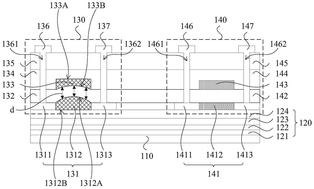
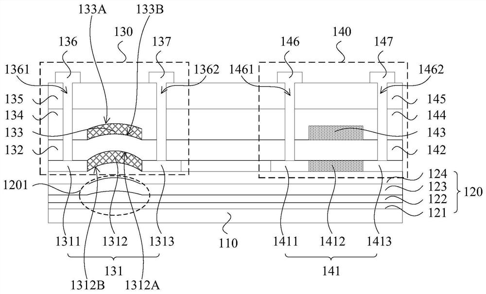
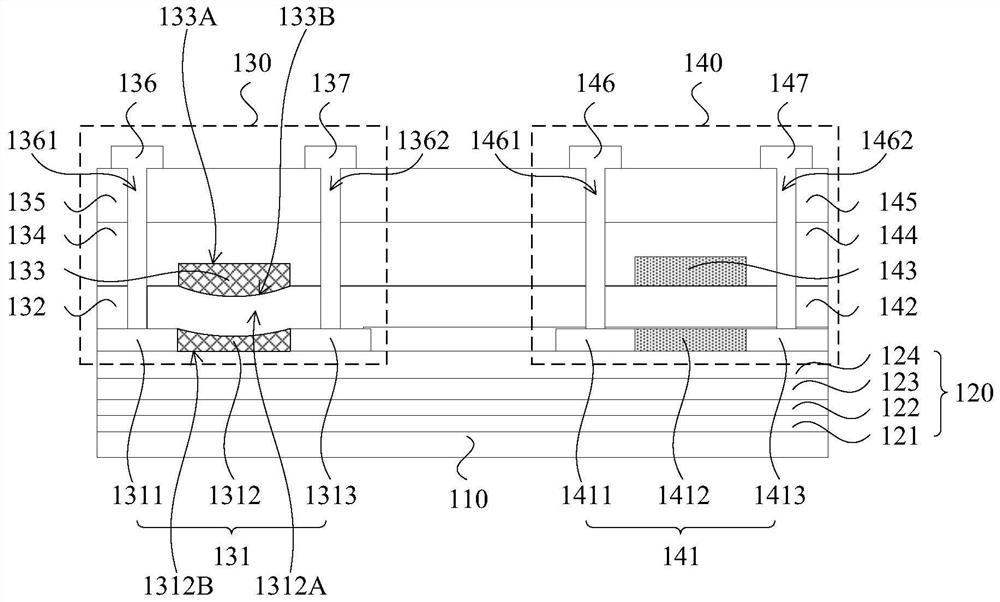
[0048] An embodiment of the present invention provides an array substrate. figure 1 A schematic structural diagram of an array substrate provided by an embodiment of the present invention. see figure 1 , the array substrate includes a first TFT 130 disposed on a substrate 110, the first TFT 130 includes a first active layer 131, a first gate insulating layer 132, and a first gate layer 133, and the first active layer 131 includes a first The channel region 1312 ; the first gate insulating layer 132 is located on...


PUM


Abstract

The embodiment of the invention discloses an array substrate and a display panel. The array substrate includes: a first thin film transistor disposed on the substrate, the first thin film transistor includes a first active layer, a first gate insulating layer and a first gate layer; wherein, the first channel of the first active layer The surface area of ​​the region close to the first gate layer is greater than the area of ​​the vertical projection of the first channel region on the substrate; the surface area of ​​the first gate layer close to the first active layer is greater than the vertical area of ​​the first gate layer on the substrate Projected area; and along the direction perpendicular to the substrate, the distances from each point on the surface of the first gate layer close to the first active layer to the surface of the first channel region close to the first gate layer are all the same. Compared with the prior art, the embodiment of the present invention improves the characteristics of the switching thin film transistor, improves the driving characteristics of the array substrate and the display effect of the display panel.

Description

technical field [0001] Embodiments of the present invention relate to the field of display technologies, and in particular, to an array substrate and a display panel. Background technique [0002] With the continuous development of display technology, display panels have been more and more widely used, and people's requirements for display panels are also getting higher and higher. [0003] The display of the existing display panel is provided with driving signals by a driving array on an array substrate. The driving array includes a large number of thin film transistors (Thin Film Transistor, TFT), one of which is a switch thin film transistor (SwitchThin Film Transistor, STFT). However, in the prior art, the characteristics of the STFT are not good, which affects the driving characteristics of the array substrate and the display effect of the display panel. Contents of the invention [0004] Embodiments of the present invention provide an array substrate and a display p...

Claims


Application Information

Patent Timeline
Patent Type & Authority Patents(China)
IPC IPC(8): H01L27/12H01L29/10H01L29/423H01L21/77H01L27/32G02F1/1362
CPCH01L27/1214H01L27/1222H01L27/1259H01L27/127H01L29/1037H01L29/42384G02F1/1362H10K59/12
Inventor 万康冯兵明顾维杰葛泳马应海
Owner YUNGU GUAN TECH CO LTD
Why Eureka
Try Eureka