
A method for manufacturing a low-melting point metal device and a method for manufacturing a solar cell

A technology of low-melting-point metals and solar cells, which is applied in semiconductor/solid-state device manufacturing, semiconductor devices, circuits, etc., and can solve problems such as damage and deformation of low-melting-point metal patterns

Active Publication Date: 2020-11-06
BEIJING DREAM INK TECH CO LTD
View PDF4 Cites 0 Cited by
  • Summary
  • Abstract
  • Description
  • Claims
  • Application Information

AI Technical Summary

Problems solved by technology

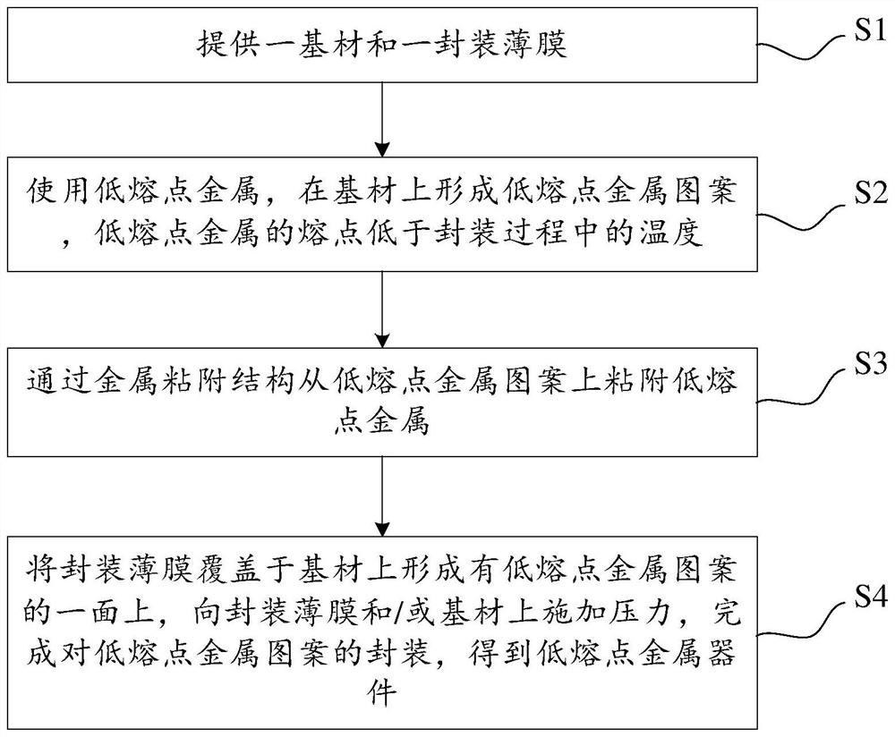
[0008] The invention provides a method for manufacturing a low-melting-point metal device and a method for manufacturing a solar cell, which can solve the problem that the low-melting-point metal pattern is deformed or damaged due to the overflow of the low-melting-point metal when the packaging film is used to package the low-melting-point metal pattern

Method used


Image

  • A method for manufacturing a low-melting point metal device and a method for manufacturing a solar cell
  • A method for manufacturing a low-melting point metal device and a method for manufacturing a solar cell
  • A method for manufacturing a low-melting point metal device and a method for manufacturing a solar cell

Examples


Embodiment Construction

[0041] In order to make the purpose, technical solutions and advantages of the embodiments of the present invention clearer, the technical solutions in the embodiments of the present invention will be clearly and completely described below in conjunction with the drawings in the embodiments of the present invention. Obviously, the described embodiments It is a part of embodiments of the present invention, but not all embodiments. Based on the embodiments of the present invention, all other embodiments obtained by persons of ordinary skill in the art without making creative efforts belong to the protection scope of the present invention.

[0042] It should be noted that the technical features in the embodiments of the present invention can be combined with each other without conflict.

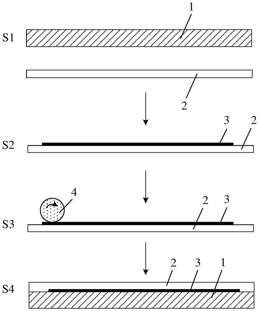
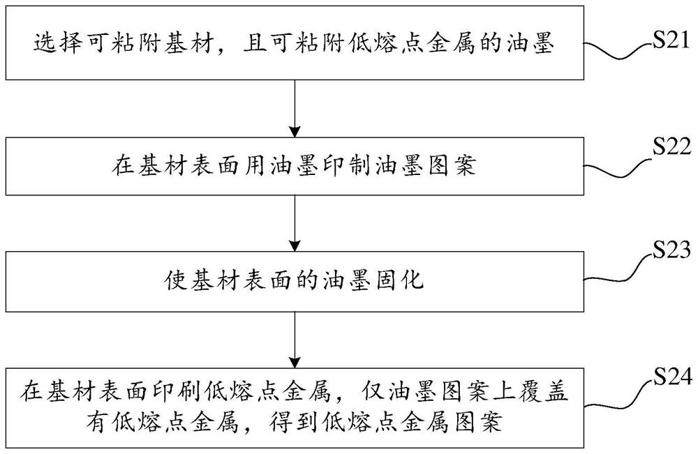
[0043] An embodiment of the present invention provides a method for manufacturing a low-melting point metal device, specifically, as figure 1 and figure 2 as shown, figure 1 A flowchart of a...


PUM

PropertyMeasurementUnit
melting pointaaaaaaaaaa
particle diameteraaaaaaaaaa

Abstract

The invention provides a manufacturing method of a low-melting-point metal device and a manufacturing method of a solar cell, and relates to the technical field of low-melting-point metal. The manufacturing method of the low-melting-point metal device comprises the steps of: providing a base material and a packaging film; adopting low-melting-point metal for forming a low-melting-point metal pattern on the base material, wherein the melting point of the low-melting-point metal is lower than the temperature in the packaging process; adhering the low-melting-point metal from the low-melting-point metal pattern through a metal adhesion structure; and covering the surface, on which the low-melting-point metal pattern is formed, of the base material with a packaging film, and applying pressureto the packaging film and / or the base material to complete packaging of the low-melting-point metal pattern, thereby obtaining the low-melting-point metal device. According to the technical scheme, the problem of deformation or damage of the low-melting-point metal pattern caused by overflow of the low-melting-point metal when the low-melting-point metal pattern is packaged by using the packagingfilm can be solved.

Description

technical field [0001] The invention relates to the technical field of low-melting-point metals, in particular to a method for manufacturing a low-melting-point metal device and a method for manufacturing a solar cell. Background technique [0002] The melting point of low-melting-point metals is lower than 300 degrees Celsius. It has the advantages of good electrical conductivity, low melting point, and good thermal conductivity. It has become an emerging functional material that has developed rapidly in recent years. In the process of applying low-melting-point metals, after the low-melting-point metal patterns are fabricated on the substrate, it is usually necessary to package the low-melting-point metal patterns to effectively protect the low-melting-point metal patterns and improve the stability of low-melting-point metal devices. [0003] At present, commonly used packaging methods include the following: [0004] The first one is to fill the uncured PDMS or silica gel...

Claims


Application Information

Patent Timeline
Patent Type & Authority Patents(China)
IPC IPC(8): H01L21/48H01L31/18
CPCH01L21/4814H01L31/18Y02P70/50
Inventor 卢双豪梁赟朱唐
Owner BEIJING DREAM INK TECH CO LTD
Learn More