Method for repairing fine line

A repair method and fine circuit technology, applied in printed circuit repair/correction, printed circuit, printed circuit, etc., can solve problems such as easy deformation and difficult circuit defects

Active Publication Date: 2020-04-07
GUANGDONG UNIV OF TECH
View PDF10 Cites 17 Cited by
  • Summary
  • Abstract
  • Description
  • Claims
  • Application Information

AI Technical Summary

Problems solved by technology

However, the texture of the bonding wire is relatively soft, and it is easy to deform under laser irradiation or during the transmission of the bonding wire, which causes certain difficulties in the operation of repairing circuit defects.

Method used


Image

  • Method for repairing fine line
  • Method for repairing fine line
  • Method for repairing fine line

Examples


Embodiment 1

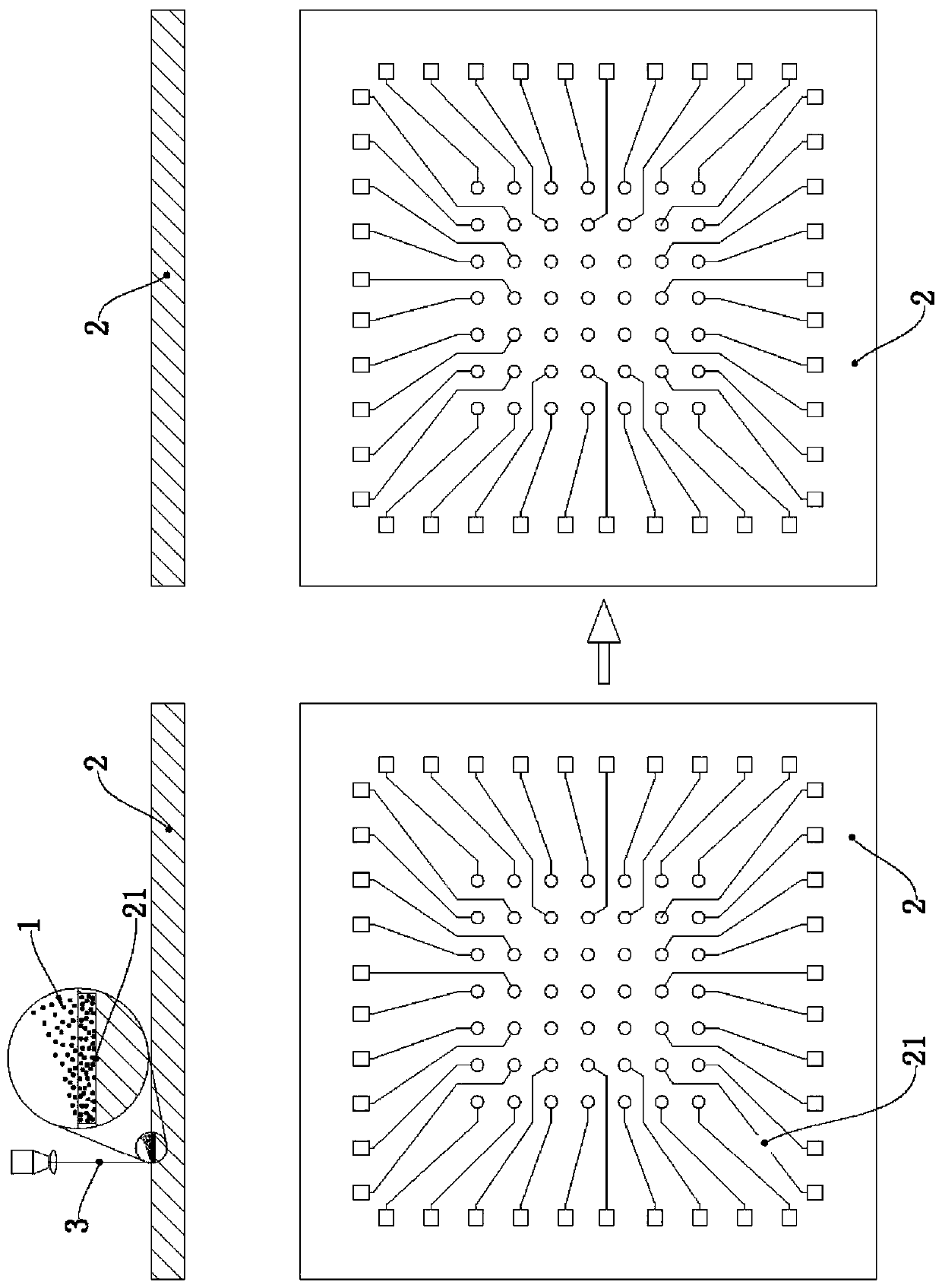
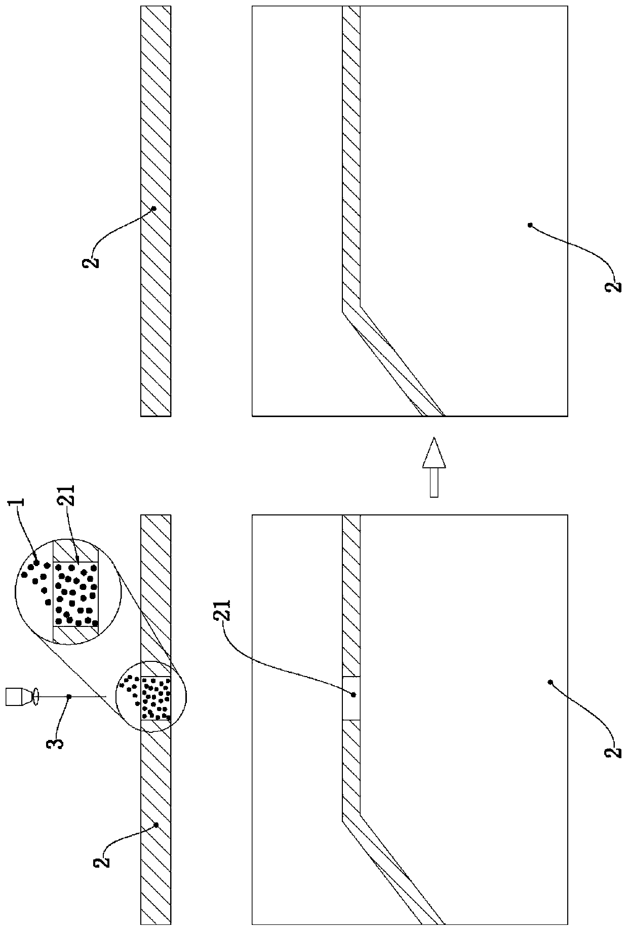
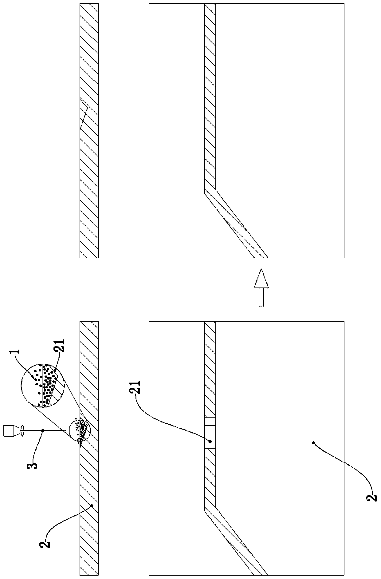
[0051] Add polyvinylpyrrolidone-coated nano-copper particles 1 with a particle size of 50nm to ethylene glycol to form a copper paste with a solid content of 80%, and drop it to a defect position 21 of a 8x8mm rewiring layer through a nozzle. The nano-copper on the line defect position 21 is irradiated by the laser 3 of appropriate wavelength and energy, and the nano-copper particle 1 melts at a relatively low temperature and fills up the line defect. After the laser 3 is removed, a conductive path is formed at the defect position, and after cleaning, the repair of the circuit defect is completed.

Embodiment 2

[0053] The imidazole-coated nano-copper particles 1 with a particle size of 100nm were added to ethylene glycol to form a copper paste with a solid content of 85%, which was dropped onto the circuit defect position 21 of the PCB board through a nozzle. The nano-copper on the line defect position 21 is irradiated by the laser 3 of appropriate wavelength and energy, and the nano-copper particle 1 melts at a relatively low temperature and fills up the line defect. After the laser 3 is removed, a conductive path is formed at the defect position, and after cleaning, the repair of the circuit defect is completed.


PUM

PropertyMeasurementUnit
particle sizeaaaaaaaaaa

Abstract

The invention discloses a method for repairing a fine circuit. The method comprises the following steps: the step A, filling nano-copper particles in a circuit defect position of a circuit board; thestep B, performing laser irradiation or direct heating on the nano-copper particles at the line defect position to enable the nano-copper particles to be metallurgically bonded with the original lineat the line defect position; and the step C, cleaning the surface of the circuit board, and removing residual nano-copper particles at an unsintered part to complete line repair. According to the invention, a fine line can be repaired, and the method has the advantage of low operation difficulty.

Description

technical field [0001] The invention relates to the technical field of integrated circuits, in particular to a repair method for fine circuits. Background technique [0002] Printed circuit board is the support body of electronic components and the carrier of electrical connection. After electronic equipment adopts printed boards, the same type of printed boards have consistency, which can reduce manual wiring errors and realize automatic insertion or installation of electronic components. Mounting, automatic soldering, and automatic detection ensure the quality of electronic equipment, improve labor productivity, reduce costs, and facilitate maintenance. With the development of miniaturization and digitalization of electronic products, printed circuit boards are also developing in the direction of high density, high precision, fine aperture, thin wire, fine pitch, high reliability, multi-layer, high-speed transmission, light weight, and thin , put forward higher requiremen...

Claims


Application Information

Patent Timeline
Patent Type & Authority Applications(China)
IPC IPC(8): H05K3/22H05K3/26
CPCH05K3/225H05K3/26H05K2203/107H05K2203/0278H05K2203/0789H05K2203/0796H05K1/097H05K2201/0272H05K3/0055H05K1/09Y10T29/49165H05K3/288H05K2203/0126H05K2203/025H05K2203/0104H05K2203/013
Inventor 崔成强杨冠南徐广东张昱陈新
Owner GUANGDONG UNIV OF TECH
Why Eureka
Try Eureka