Workpiece caching device, device front-end module and semiconductor device

A front-end module of equipment, semiconductor technology, applied in semiconductor/solid-state device manufacturing, electrical components, conveyor objects, etc., can solve problems such as large contact area between the card slot and the wafer, scratches and wear on the back of the wafer, and large impact , to reduce the possibility of pollution and damage, the effect of the original structure is small, and the installation method is simple

Pending Publication Date: 2020-04-10
BEIJING NAURA MICROELECTRONICS EQUIP CO LTD
View PDF6 Cites 0 Cited by
  • Summary
  • Abstract
  • Description
  • Claims
  • Application Information

AI Technical Summary

Problems solved by technology

[0004] (1) A loading position 03 of the front-end module 01 of the equipment is occupied, which is not only difficult to implement and high in cost, but also reduces the number of loading positions 03, which has a greater impact on the front-end module 01 of the entire equipment;
[0005] (2) Since the loading position 03 is outside the front-end module 01 of the equipment, it is not conducive to the movement of the positive and negative charges generated by the clean airflow of the fan filter unit and the ion bar to this place, so the wafer environment in the wafer buffer device 02 is difficult to ensure that it is consistent with the equipment The interior of the front-end module 01 is consistent, and it is not conducive to the electrostatic discharge of the wafer;
[0006] (3) The contact area between the card slot and the wafer is large, and the processing of the card slot is difficult, and its surface is not smooth enough, which may easily cause scratches and wear on the back of the wafer

Method used


Image

  • Workpiece caching device, device front-end module and semiconductor device
  • Workpiece caching device, device front-end module and semiconductor device
  • Workpiece caching device, device front-end module and semiconductor device

Examples


Embodiment Construction

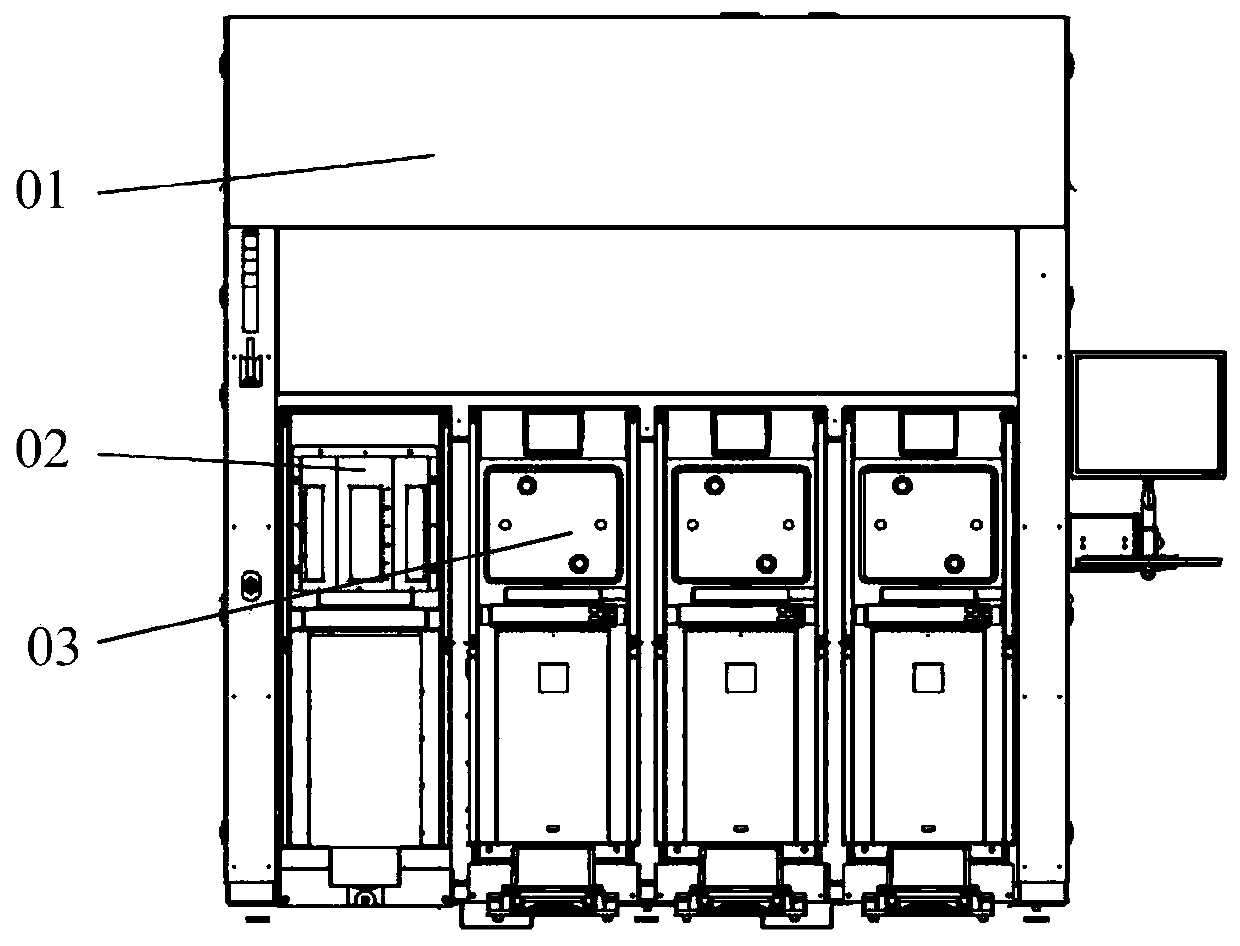
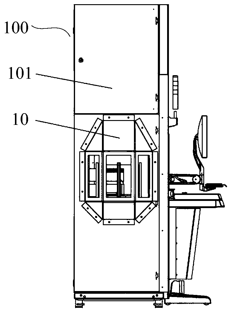
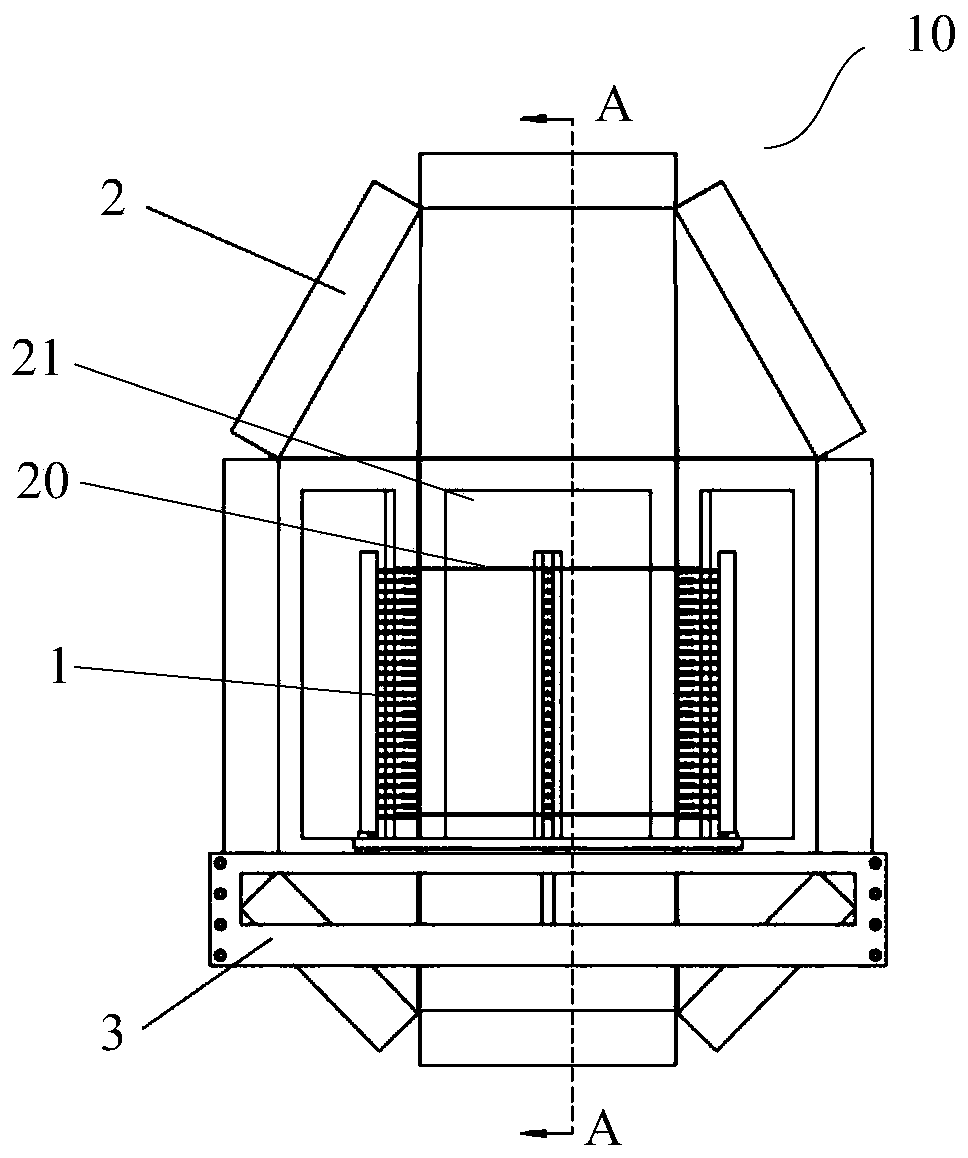
[0037] The present application is described in detail below, and examples of embodiments of the present application are shown in the drawings, wherein the same or similar reference numerals denote the same or similar components or components having the same or similar functions throughout. Also, detailed descriptions of known technologies will be omitted if they are not necessary to illustrate the features of the present application. The embodiments described below by referring to the figures are exemplary only for explaining the present application, and are not construed as limiting the present application.

[0038] Those skilled in the art can understand that, unless otherwise defined, all terms (including technical terms and scientific terms) used herein have the same meanings as commonly understood by those of ordinary skill in the art to which this application belongs. It should also be understood that terms, such as those defined in commonly used dictionaries, should be ...


PUM


Abstract

The invention provides a workpiece caching device, a device front-end module and a semiconductor device. The workpiece caching device is hung on the outer wall of the device front-end module, is communicated with the internal space of the device front-end module and comprises a bearing assembly, a fixing assembly and a shell, wherein the shell is connected with the outer wall of the device front-end module in a sealed mode, a containing space capable of containing the bearing assembly is formed in the shell, and the containing space is communicated with the internal space of the device front-end module; the bearing assembly is used for bearing a cache workpiece; the fixing assembly is used for fixing the bearing assembly in the containing space. According to the present invention, the workpiece caching is achieved, the original loading position of the device front-end module is not occupied, the influence on the original structure of the device front-end module is smaller, the implementation is easier, and the cost is lower; the electrostatic charge on the surface of the cache workpiece can be eliminated, the cleanliness of the environment where the cache workpiece is located is ensured, and the possibility that the cache workpiece is polluted and damaged is effectively reduced.

Description

technical field [0001] The invention relates to the technical field of semiconductors, in particular to a workpiece buffer device, a front-end module of equipment and semiconductor equipment. Background technique [0002] In semiconductor equipment, a wafer cache device is usually added to the hardware equipment (such as the equipment front-end module of the process equipment) to cache the wafers (such as wafers) that have been processed, so as to prevent the caching of wafers and unprocessed wafers. Wafers are placed in the same load port at the same time, which prevents particles attached to buffered wafers from contaminating unprocessed wafers. [0003] Currently, if figure 1 As shown, the wafer buffer device 02 occupies a loading position 03, and is installed on the front-end module 01 of the equipment by using the installation interface of the original loading position 03. The wafer buffer device 02 includes a base and a plurality of brackets arranged on the base. The...

Claims


Application Information

Patent Timeline
IPC IPC(8): H01L21/67H01L21/677
CPCH01L21/67161H01L21/67742
Inventor 侯文潭李莉
Owner BEIJING NAURA MICROELECTRONICS EQUIP CO LTD
Why Eureka
Try Eureka