Array substrate, display panel and manufacturing method of array substrate

A technology of an array substrate and a manufacturing method, which are applied in the manufacture of display panels and array substrates, and the field of array substrates, can solve the problems of high contact resistance of conductive layers, etc., so as to improve the yield rate of panels, improve the yield rate of products, and reduce the limitation of circuit space. Effect

Inactive Publication Date: 2020-04-10
SHENZHEN CHINA STAR OPTOELECTRONICS TECH CO LTD
View PDF4 Cites 1 Cited by
  • Summary
  • Abstract
  • Description
  • Claims
  • Application Information

AI Technical Summary

Problems solved by technology

[0007] The embodiment of the present application provides an array substrate, a display panel, and a method for manufacturing the array substrate. By improving the deep and shallow hole via technology, the problem of large contact resistance of the conductive layer at the deep and shallow hole can be solved, and the first metal layer at the deep and shallow hole can be reduced. Contact resistance with the second metal layer, improve product yield, improve display quality

Method used


Image

  • Array substrate, display panel and manufacturing method of array substrate
  • Array substrate, display panel and manufacturing method of array substrate
  • Array substrate, display panel and manufacturing method of array substrate

Examples


Embodiment Construction

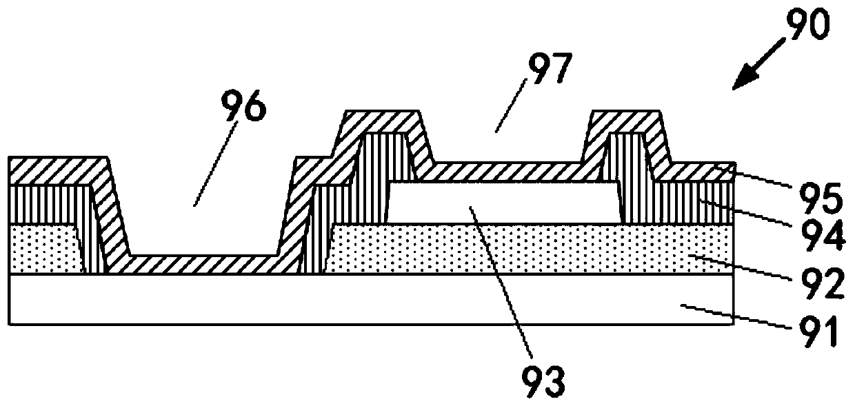
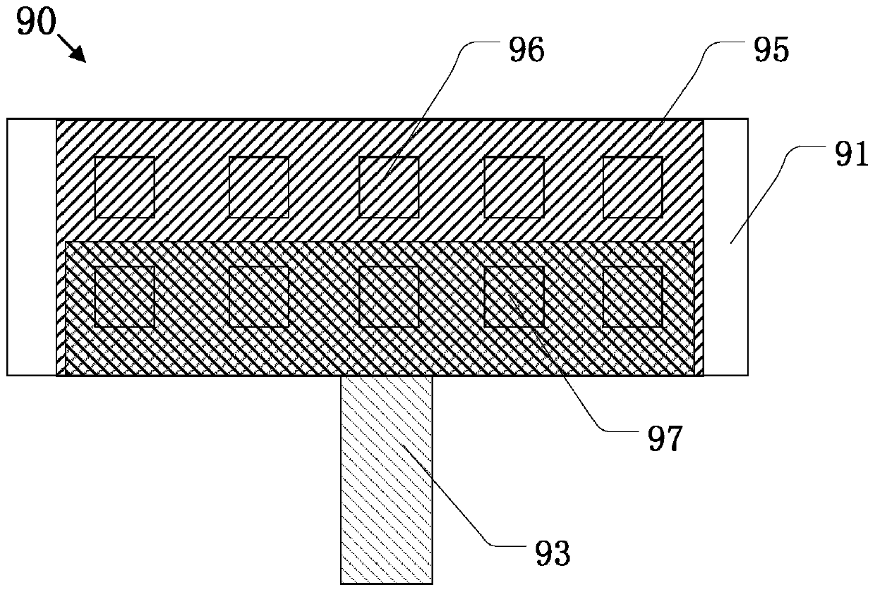
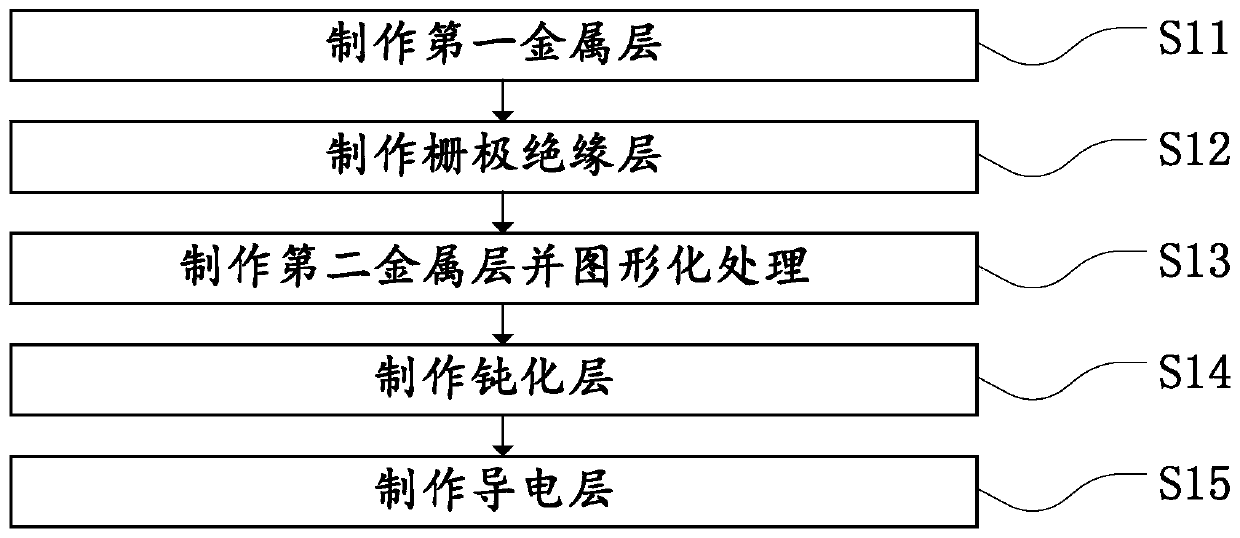
[0045] The technical solutions in the embodiments of the present application will be clearly and completely described below in conjunction with the drawings in the embodiments of the present application. Apparently, the described embodiments are only some of the embodiments of this application, not all of them. Based on the embodiments in this application, all other embodiments obtained by those skilled in the art without making creative efforts belong to the scope of protection of this application.

[0046] In the description of the present application, it should be understood that the terms "center", "longitudinal", "transverse", "length", "width", "thickness", "upper", "lower", "front", " Orientation indicated by rear, left, right, vertical, horizontal, top, bottom, inside, outside, clockwise, counterclockwise, etc. The positional relationship is based on the orientation or positional relationship shown in the drawings, which is only for the convenience of describing the a...


PUM

PropertyMeasurementUnit
angleaaaaaaaaaa

Abstract

The invention discloses an array substrate, a display panel and a manufacturing method of the array substrate. The array substrate is provided with a row driving region, and the row driving region comprises a first metal layer, a gate insulating layer and a second metal layer; the gate insulating layer is located on the first metal layer, and the gate insulating layer is provided with a through hole; and the second metal layer is located on the gate insulating layer and extends to the inner side wall of the first through hole and the surface of the first metal layer corresponding to the through hole. Impedance is reduced through direct contact between the first metal layer and the second metal layer, so that hole burning abnormity is not liable to occur, and the panel yield and the panel reliability are improved; and moreover, the number of through holes in the gate insulating layer can be relatively reduced, the circuit space limitation of the row driving region is reduced, and a narrow frame is favorably realized.

Description

technical field [0001] The present application relates to the technical field of mobile communication, in particular to the technical field of mobile devices, and in particular to an array substrate, a display panel and a method for manufacturing the array substrate. Background technique [0002] At present, the design of array substrate row driver (GOA) circuit has been generalized. figure 1 It is a structural schematic diagram of an existing array substrate. The array substrate 90 in the row driving area includes a first metal layer 91, a gate insulating layer 92, a second metal layer 93, a passivation layer 94 and a conductive layer 95 stacked. . In order to realize the conduction between the first metal layer 91 and the second metal layer 93 to transmit electrical signals, it is usually necessary to set separated first via holes 96 and second via holes 97 and cover them with a conductive layer 95 to conduct the first metal layer 91 and the second via hole 97. The secon...

Claims


Application Information

Patent Timeline
Patent Type & Authority Applications(China)
IPC IPC(8): H01L27/12H01L21/77
CPCH01L27/124H01L27/1259
Inventor 孙正娟
Owner SHENZHEN CHINA STAR OPTOELECTRONICS TECH CO LTD
Why Eureka
Try Eureka